SLAAED9 November 2023 TAA5412-Q1 , TAC5311-Q1 , TAC5312-Q1 , TAC5411-Q1 , TAC5412-Q1
- 1
- Abstract
- Trademarks
- 1 Introduction
- 2 Diagnostic Monitoring Architecture
- 3 Monitored Faults
- 4 Enabling Diagnostics and Programming Thresholds
- 5 Fault Diagnostic Setup Procedure
-
6 Fault Reporting
- 6.1
Live Registers
- 6.1.1 CHx_LIVE Register (page = 0x01, address = 0x3D) [Reset = 0b]
- 6.1.2 CH1_LIVE Register (page = 0x01, address = 0x3E) [Reset = 0h]
- 6.1.3 INT_LIVE0 Register (page = 0x01, address = 0x3C) [Reset = 00]
- 6.1.4 INT_LIVE1 Register (page = 0x00, address = 0x42) [reset = 0x00]
- 6.1.5 INT_LIVE2 Register (page = 0x00, address = 0x43) [reset = 0x00]
- 6.2 Latched Registers
- 6.3 Fault Filtering and Response Time
- 6.1
Live Registers
- 7 Responding to a Fault
- 8 Using PurePath Console
- 9 Diagnostic Monitoring Registers
- 10Summary
- 11References
3.2.2 Virtual Ground
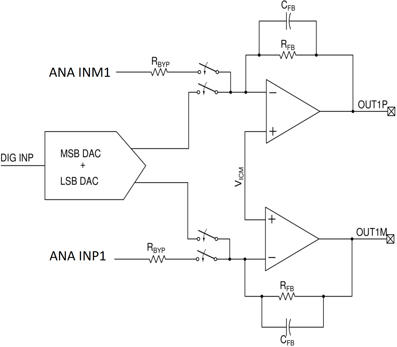
Preceding the output pins is an amplifier operating at AVDD that creates a midpoint voltage to serve as a reference point for the analog input signal. This midpoint voltage, shown as V_ICM (which stands for "internal common-mode") in Figure 3-8, is referred to as the virtual ground. A fault is triggered if there is a short at OUTx that brings the virtual ground to unintended high voltages. Furthermore, a fault can be triggered under the following conditions:
- If the analog input signal common mode is higher than 100 mV, thus breaking the limitation of RBYP and bringing the virtual ground to unintended high voltages. This is only applicable when the device output configuration is fully-differential.
- If the device is configured to have a 6-db or 12-dB gain in bypass and the input signal is greater than -6-dB or -12-dB respectively. This is applicable to single-ended or fully-differential output configurations.
- If the analog input level exceeds the full scale input signal range for the respective input configuration.
Correct configuration of the output registers for channel 1 (P0_R100-R102) and channel 2 (P0_R107-R109) is essential to prevent unintended virtual ground fault detection. In the event a virtual ground fault is detected, the user must check the output configuration registers and verify compliance with the input signal and voltages.
In addition, the DAC output stage is shown in Figure 3-8 and if the voltage measured at OUTx exceeds the design limits of the device, this fault triggers. The user has the ability to program the device in DAC_FLT_CFG (P0_R67) to power down the playback path of the DAC upon fault detection.
 Figure 3-8 Virtual Ground Output Configuration