SLAAEF9 November   2023 MSPM0L1306


  1.   1
  2.   Abstract
  3.   Trademarks
  4. 1MSPM0 Portfolio Overview
    1. 1.1 Introduction
    2. 1.2 Portfolio Comparison of Renesas RL78 MCUs to MSPM0 MCUs
  5. 2Ecosystem And Migration
    1. 2.1 Ecosystem Comparison
      1. 2.1.1 MSPM0 Software Development Kit (MSPM0 SDK)
      2. 2.1.2 The IDE Supported By MSPM0
      3. 2.1.3 SysConfig
      4. 2.1.4 Debug Tools
      5. 2.1.5 LaunchPad
    2. 2.2 Migration Process
      1. 2.2.1 Step 1. Choose The Right MSPM0 MCU
      2. 2.2.2 Step 2. Set Up IDE And Quick Introduction of CCS
        1. 2.2.2.1 Set Up IDE
        2. 2.2.2.2 Quick Introduction of CCS
      3. 2.2.3 Step 3. Set Up MSPM0 SDK And Quick Introduction of MSPM0 SDK
        1. 2.2.3.1 Set Up MSPM0 SDK
        2. 2.2.3.2 Quick Introduction of SDK
      4. 2.2.4 Step 4. Software Evaluation
      5. 2.2.5 Step 5. PCB Board Design
      6. 2.2.6 Step 6. Mass Production
    3. 2.3 Example
  6. 3Core Architecture Comparison
    1. 3.1 CPU
    2. 3.2 Embedded Memory Comparison
      1. 3.2.1 Flash Features
      2. 3.2.2 Flash Organization
        1. 3.2.2.1 Flash Memory Regions
        2. 3.2.2.2 NONMAIN Memory of MSPM0
        3. 3.2.2.3 Flash Memory Registers of RL78
      3. 3.2.3 Embedded SRAM
    3. 3.3 Power UP and Reset Summary and Comparison
    4. 3.4 Clocks Summary and Comparison
      1. 3.4.1 Oscillators
        1. 3.4.1.1 MSPM0 Oscillators
      2. 3.4.2 Clock Signal Comparison
    5. 3.5 MSPM0 Operating Modes Summary and Comparison
      1. 3.5.1 Operating Modes Comparison
      2. 3.5.2 MSPM0 Capabilities in Lower Modes
      3. 3.5.3 Entering Lower-Power Modes
      4. 3.5.4 Low-Power Mode Code Examples
    6. 3.6 Interrupts and Events Comparison
      1. 3.6.1 Interrupts and Exceptions
        1. 3.6.1.1 Interrupt Management of RL78
        2. 3.6.1.2 Interrupt Management of MSPM0
      2. 3.6.2 Event Handler of MSPM0
      3. 3.6.3 Event Link Controller (ELC) of RL78
      4. 3.6.4 Event Management Comparison
    7. 3.7 Debug and Programming Comparison
      1. 3.7.1 Debug Comparison
      2. 3.7.2 Programming Mode Comparison
        1. 3.7.2.1 Bootstrap Loader (BSL) Programming of MSPM0
        2. 3.7.2.2 Serial Programming (Using External Device) of RL78
  7. 4Digital Peripheral Comparison
    1. 4.1 General-Purpose I/O (GPIO, IOMUX)
    2. 4.2 Universal Asynchronous Receiver-Transmitter (UART)
    3. 4.3 Serial Peripheral Interface (SPI)
    4. 4.4 Inter-Integrated Circuit (I2C)
    5. 4.5 Timers (TIMGx, TIMAx)
    6. 4.6 Windowed Watchdog Timer (WWDT)
    7. 4.7 Real-Time Clock (RTC)
  8. 5Analog Peripheral Comparison
    1. 5.1 Analog-to-Digital Converter (ADC)
    2. 5.2 Comparator (COMP)
    3. 5.3 Digital-to-Analog Converter (DAC)
    4. 5.4 Operational Amplifier (OPA)
    5. 5.5 Voltage References (VREF)

Step 5. PCB Board Design

  1. To get the design package, go through the Ti.com and enter the specific device page. Take MSPM0L1304, for example.
  2. Click Design and development --> CAD/CAE symbols, select different package models to download according to your needs.
    GUID-50CE7D6C-D4DB-48E9-913D-B9BB794D2468-low.png Figure 2-39 Ultra Librarian Tool Entrance
  3. As for MSPM0 hardware design into your own board. Figure 2-40 shows a sample minimal system design.
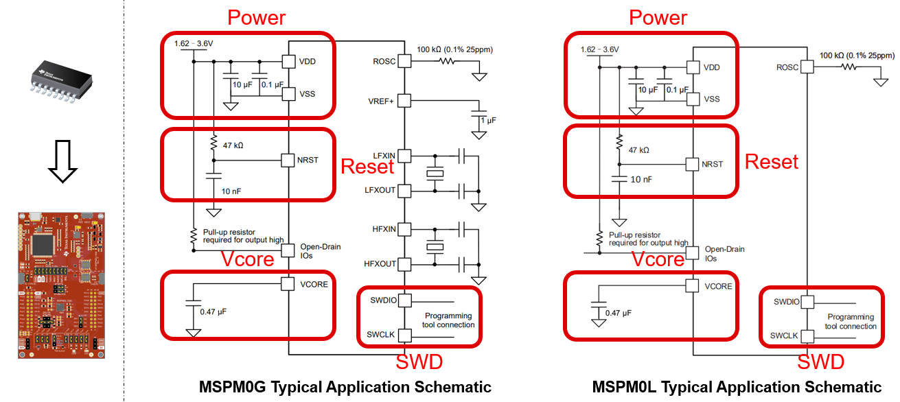
    GUID-E1DB5491-2E98-45E4-BA58-D9F493A968AA-low.png Figure 2-40 MSPM0 Minimum System

    For minimal systems, the following points need to be noted:
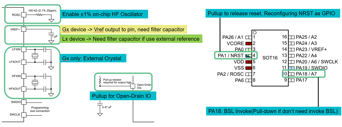
    GUID-39862D56-0B0E-4B2A-9097-766D7610C069-low.png Figure 2-41 MSPM0 Minimum System Attention

    For more detailed information about hardware development, see the following: