SLAAEJ1 March 2024 MSPM0L1306
Design Description
Many applications need to capture status change of several GPIOs at the same time, update, and then send the status to host through UART. Cost-effective microcontroller (MCU) with enough GPIO resource can implement parallel-to-serial and send data through UART to host, for example PC side, in real time. Download the code for this example.
Figure 1-1 shows a functional diagram of this subsystem.
 Figure 1-1 Subsystem Functional Block
Diagram
Figure 1-1 Subsystem Functional Block
DiagramRequired Peripherals
This application requires 9 GPIO, 1 timers, and 1 UART.
| Sub-block Functionality | Peripheral Use | Notes |
|---|---|---|
| IO input | 9 pins | Called GROUP1_IRQHandler in code |
| Timer interval | TIMG0 | Called TIMG0_IRQHandler in code |
| UART output | UART0 | Called transmitPacketBlocking in code |
Compatible Devices
Based on the requirements in Table 1-1, this example is compatible with the devices in Table 1-2. The corresponding EVM can be used for prototyping.
| Compatible Devices | EVM |
|---|---|
| MSPM0L1xx | LP-MSPM0L1306 |
| MSPM0G3xx/1xx | LP-MSPM0G3507 |
Design Steps
- Capture 9 GPIO switches’ status.
- Fill these 9 bits in data segment and transmit one completed frame to host PC through UART.
- Update the data when any operation is detected or every 40ms.
Design Considerations
This implementation uses 9 GPIO Pins (PA10-PA18) to capture the switches’ status represented the corresponding operations shown in Table 1-3:
| GPIO Pins | Operations |
|---|---|
| PA10 | GPIO_Signal_10 |
| PA11 | GPIO_Signal_11 |
| PA12 | GPIO_Signal_12 |
| PA13 | GPIO_Signal_13 |
| PA14 | GPIO_Signal_14 |
| PA15 | GPIO_Signal_15 |
| PA16 | GPIO_Signal_16 |
| PA17 | GPIO_Signal_17 |
| PA18 | GPIO_Signal_18 |
In the above pins, PA14 is connected to S2 fixedly in Launch Pad and when S2 is pressed, PA14 is pulled down to Ground. For the other pins, each pin can be connected to S1 through J11 and when S1 is pressed, the pin can be pulled up to 3V3. For example, if the S1 is connected to PA18 and both SWs is pressed at same time, the data updates shown in Table 1-4:
| Bit15 | Bit14 | Bit13 | Bit12 | Bit11 | Bit10 | Bit9 | Bit8 | Bit7 | Bit6 | Bit5 | Bit4 | Bit3 | Bit2 | Bit1 | Bit0 | |
|---|---|---|---|---|---|---|---|---|---|---|---|---|---|---|---|---|
| GPIO Pin | PA18 | PA17 | PA16 | PA15 | PA14 | PA13 | PA12 | PA11 | PA10 | |||||||
| Default | 0 | 0 | 0 | 0 | 0 | 0 | 0 | 0 | 0 | 0 | 0 | 1 | 0 | 0 | 0 | 0 |
| PA18&14 | 0 | 0 | 0 | 0 | 0 | 0 | 0 | 1 | 0 | 0 | 0 | 0 | 0 | 0 | 0 | 0 |
When any SW is pressed, MCU can update the data segment (2 Bytes) and check sum immediately and send the new data, which is composed in the following format, through UART to PC.
If no SW is pressed for every 40ms, MCU can send the current status to PC. The package sent to PC has the format shown in Table 1-5:
| Bytes | Header (2Byte) | Data Length (1Byte) | Source ID (1Byte) | Destination ID (1Byte) | Command (1Byte) | Data index (1Byte) | Data (N Byte) | Checksum (2Byte) | ||
|---|---|---|---|---|---|---|---|---|---|---|
| Value | 0x5A | 0xA5 | N | 0~63 | 0~63 | 0~255 | 0~255 | Data | CSumL | CSumH |
Software Flowchart
Figure 1-2 shows the code flow diagram of main loop which is main function and GPIO interrupt handling which is GROUP1_IRQHandler function.
TIMG0 interrupt handling is very simple which is entering Timer interrupt and send current data every 40ms, Figure 1-2 Application Software
Flowchart
Figure 1-2 Application Software
FlowchartApplication code
Main loop
    SYSCFG_DL_init();
    NVIC_EnableIRQ(GPIO_MULTIPLE_GPIOA_INT_IRQN);
    NVIC_EnableIRQ(TIMER_0_INST_INT_IRQN);
    DL_TimerG_startCounter(TIMER_0_INST);
    while (1) {
        __WFI();
}
TIMG0_IRQHandler
    switch (DL_TimerG_getPendingInterrupt(TIMER_0_INST)) {
        case DL_TIMER_IIDX_ZERO:
            transmitPacketBlocking(gTxPacket,UART_PACKET_SIZE);
            break;
GPIO GROUP1_IRQHandler
    if (DL_Interrupt_getPendingGroup(DL_INTERRUPT_GROUP_1)) {

        dataStatus = (GPIOA->DIN31_0);
        dataTemp = (dataStatus >> 10);
        gTxPacket[7] = dataTemp >> 8;
        gTxPacket[8] = dataTemp & 0xFF;

        siganlChecksum = checkSum1ByteIn2ByteOut((gTxPacket+2),7);

        gTxPacket[10] = siganlChecksum >> 8;
        gTxPacket[9] = siganlChecksum & 0xFF;

        DL_TimerG_stopCounter(TIMER_0_INST);
        DL_TimerG_setTimerCount(TIMER_0_INST,TIMER_0_INST_LOAD_VALUE);
        DL_TimerG_startCounter(TIMER_0_INST);

        transmitPacketBlocking(gTxPacket,UART_PACKET_SIZE);
}
Results
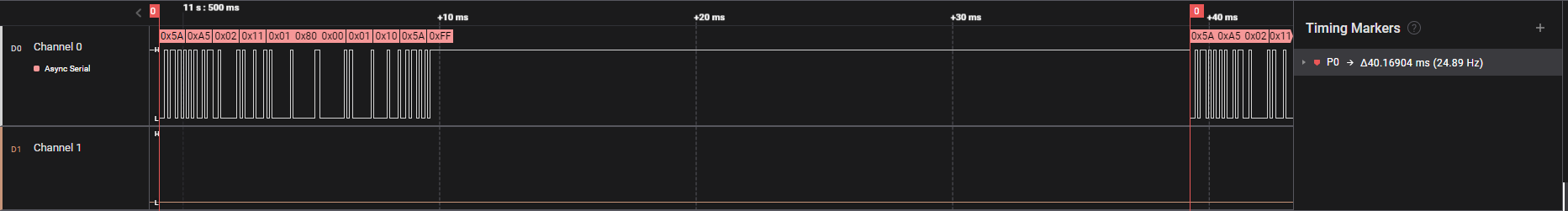
Using Logical Analysis to capture data flow and show more details.
Channel 0 ----> UART Tx
Channel 1 ----> PA18
The following images show:
When no SWs pressed, MCU sends default value every 40ms
When S1 is pressed, PA18 occurs rising edge and data update. Then MCU sends the update data every 40ms.
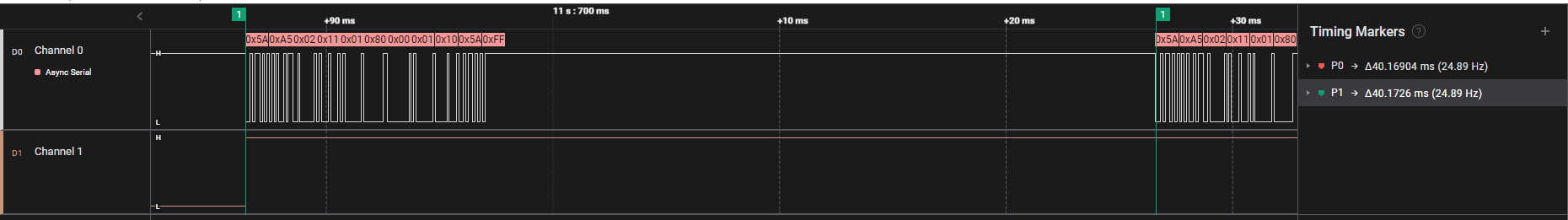
If the rising edge occurs, but the last package has not been finished, MCU sends a data update after the last transmission is accomplished.
