SLAAEO3 September   2024 MSPM0L2227 , MSPM0L2228


  1.   1
  2.   Abstract
  3.   Trademarks
  4. 1Introduction: MSPM0 and LCD End Applications
  5. 2MSPM0 LCD Portfolio
  6. 3Segmented LCD Operation
    1. 3.1 LCD Structure (Simplified)
    2. 3.2 LCD Drive Basics
  7. 4MSPM0 LCD Features
    1. 4.1 Muxing
      1. 4.1.1 Muxing Example
    2. 4.2 Voltage Generation
      1. 4.2.1 Charge Pump
      2. 4.2.2 Contrast Control
    3. 4.3 LCD Clocking
    4. 4.4 LCD Memory and Blinking Mode
      1. 4.4.1 LCD Memory Organization
      2. 4.4.2 Blinking
    5. 4.5 LCD Output Pin Configuration
    6. 4.6 Low Power Mode Feature
  8. 5LCD Layout and Software Considerations
    1. 5.1 LCD Layout Tips
      1. 5.1.1 Hardware-Driven Layout
      2. 5.1.2 Software-Driven Layout
      3. 5.1.3 General Layout Rules
    2. 5.2 LCD Software Tips
      1. 5.2.1 Create a Look-up Table
      2. 5.2.2 Use of #defines
      3. 5.2.3 Efficient Clearing of the LCD Memory
      4. 5.2.4 Double-buffering of the Display Buffer Using Dual Display Memory
  9. 6Additional Resources

Muxing Example

Figure 4-2 shows a 4-mux 1/3 bias waveform. Each segment is controlled by signals on 2 pins – a COMx pin and an Sx segment pin. The signals shown are the waveforms applied on the electrodes for the segment, so the potential difference between the Sx and COMx signal is what is applied to the liquid crystals in that area. This potential difference is what is shown as the voltage in the resultant waveforms in Figure 4-2 (COM0-S0 and COM1-S1).

In this example, the COM0-S0 waveform has a high RMS voltage so the segment is on even though the waveform has a net zero DC voltage. The COM1-S1 waveform has a low RMS voltage, so the segment is off. While the waveforms look complex, they are generated automatically by the MSPM0 LCD module – the user only specifies the basic settings of the LCD and indicates which segments is on or off.
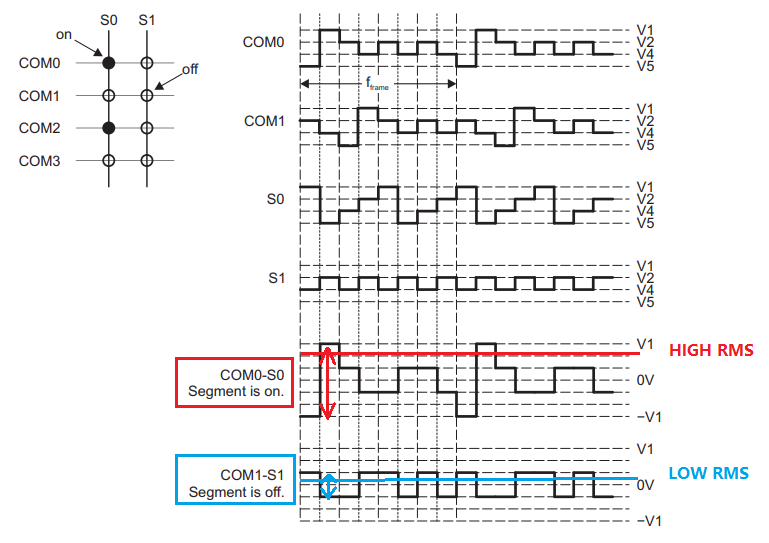
MSPM0L222x 4-Mux 1/3 Bias Figure 4-2 4-Mux 1/3 Bias