SLAAEO3 September 2024 MSPM0L2227 , MSPM0L2228
5.1.3 General Layout Rules
LCD signal lines are constantly switching to keep the image on the display, keep them away from noise-sensitive lines (like the external crystal connections). Use guard rings to shield noise-sensitive lines, like the crystal connections or ADC inputs, from noise coupling. A ground plane underneath the LCD traces and guard traces also provide shielding.
One good practice is to keep all LCD signal traces (segment and common lines) together, similar to a data bus. Keeping the LCD layout in a single layer is helpful so that there are not LCD traces running over or under potentially sensitive traces. Keep the charge pump capacitor on the LOADCAP pin as close as possible to the MCU with a short trace.
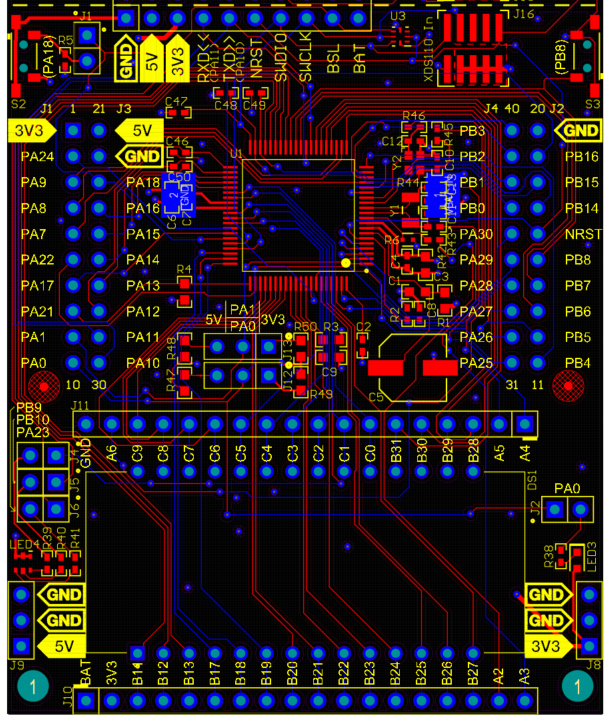
Figure 5-4 shows a portion of the water meter design showing the LCD connections. The signals to the LCD at the top of the layout are grouped together and go around the crystal oscillators X1 and X2 rather than under to prevent noise from disturbing the crystals. The crystal circuitry also includes its own ground plane to help further shield them from noise from the LCD and other sources.
 Figure 5-4 Portion of LP-MSPM0L2228
Design Showing LCD Layout