SLAAEO3 September 2024 MSPM0L2227 , MSPM0L2228
5.1.2 Software-Driven Layout
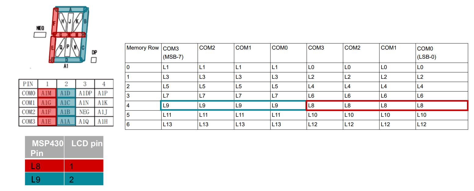
Using a software-driven approach for pin selection allows the MSPM0 to set all required segments to display digits and characters using a single memory write of a byte or word. For example, for the 4-mux display shown previously in Figure 5-1, two pins control all the segments to display any digit 0-9, and four pins control all the segments to display any alphanumeric character. In 4-mux mode, the MSPM0 LCD memory has each byte controlling two Sx pins. Therefore, with careful connections between the MSPM0 and this LCD glass, set on a display is a full digit with a single byte access (writing two pins at once), or a full alphabet character is on the display with a half-word access (writing four pins at once). Figure 5-3 shows an example of choosing MSPM0 Sx pins within the same LCDMx memory register so that all segments for both Sx pins are set with a single byte access. It is also important to make sure that the same segments for each digit are assigned to the same ordering within the byte and are laid out in the same format in memory to confirm that the same function call is used, no matter the set digit of the display, saving greatly on software overhead.
However, depending on the application, the connections are more complex or require a multilayered board. On devices with LCD module, any pin is a COM pin or a segment pin helping to make layout easier which helps to mitigate the layout issue to an extent.
 Figure 5-3 Software-Driven Layout Pin Selection
Example