SLAAEO3 September 2024 MSPM0L2227 , MSPM0L2228
4.2 Voltage Generation
There are 5 levels (V1, V2, V3, V4, V5) of voltages used to generate different waveforms on segment and common pins, depending on the bias mode. Check the voltage level in different bias mode in Table 4-1.
| Voltage Level | Static | 1/3 bias mode | 1/4 bias mode |
|---|---|---|---|
| V1(VLCD) | VLCD | VLCD | VLCD |
| V2 | NA | VLCD × 2/3 | VLCD × 3/4 |
| V3 | NA | NA | VLCD × 1/2 |
| V4 | NA | VLCD × 1/3 | VLCD × 1/4 |
| V5 | 0 | 0 | 0 |
The highest voltage level V1 is generated by VLCD. VLCD is sourced externally or from the internal charge pump, as discussed in Section 4.2.1. To produce the rest of the voltage levels in the LCD waveforms V2 through V5, the module produces bias voltages at fractions of VLCD.
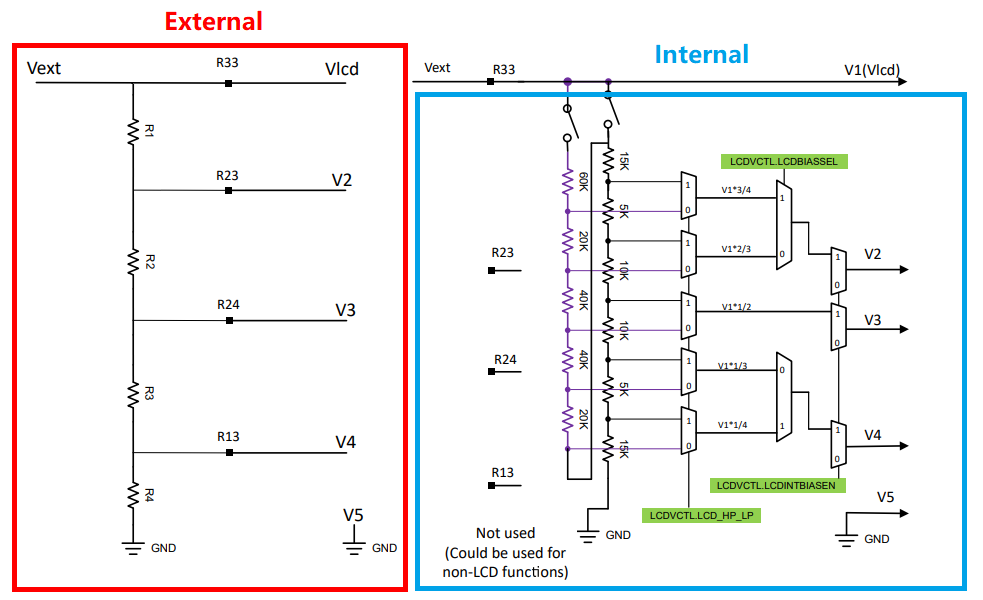
Divide the bias voltages V2 through V5 down from VLCD internally or with an external resistor network. Customer can choose to use any combination of the source of VLCD and the bias voltage generation method in their application. Table 4-2 shows an example of the possible internal and external bias options with different source of VLCD in one of the LCD modules.
| Mode | Description |
|---|---|
| 0 | Voltage generation from external reference and external resistor divider |
| 1 | Voltage generation from AVDD and external resistor divider |
| 2 | Voltage generation from external reference and internal resistor divider |
| 3 | Voltage generation from AVDD and internal resistor ladder |
| 4 | Voltage generation from charge pump with external supply |
| 5 | Voltage generation from charge pump with AVDD |
| 6 | Voltage generation from charge pump with external reference on R13 |
| 7 | Voltage generation from charge pump with internal reference on R13 |
Generating bias voltages internally is simple because no external components are required – the module internally divides down the voltage. However, generating bias voltages externally instead may be lower power. External biasing requires the user to provide an external resistor divider to create the voltages V2 through V5 - the resistor divider used depends on the biasing mode – static, 1/3, or 1/4 bias, as shown in Figure 4-3. The resistors in the divider must all be the same value, but the size used may depend on the particular display used in the design.
Changing the external resistor values impacts both current consumption and contrast. Larger resistors cause less current consumption in the resistor ladder, saving power. However, if resistors are too large, the contrast may not be good or even for all segments. Experimentation with different sizes of resistor is usually needed in a design to find the best combination of performance versus current consumption.
 Figure 4-3 Voltage Generation
Configurations