SLAU472C February 2013 – November 2023 TAS2505 , TAS2505-Q1
- 1
- Trademarks
- 1 TAS2505 Device Overview
- 2Description
-
3
TAS2505 Application
- 3.1 Terminal Descriptions
- 3.2 Audio Analog I/O
- 3.3 Analog Signals
- 3.4
Audio DAC and Audio Analog Outputs
- 3.4.1 DAC
- 3.4.2 DAC Gain Setting
- 3.4.3 Interrupts
- 3.4.4 Programming DAC Digital Filter Coefficients
- 3.4.5 Updating DAC Digital Filter Coefficients During PLAY
- 3.4.6 Digital Mixing and Routing
- 3.4.7 Analog Audio Routing
- 3.4.8 Analog Outputs
- 3.4.9 Audio Output-Stage Power Configurations
- 3.4.10 5V LDO
- 3.4.11 POR
- 3.4.12 DAC Setup
- 3.5
PowerTune
- 3.5.1 PowerTune Modes
- 3.5.2 DAC Power Consumption
- 3.5.3
Speaker output Power Consumption
- 3.5.3.1 Speaker output, Mono, 48 kHz, Highest Performance, DVDD = IOVDD = 1.8 V, AVDD = 1.8 V, SPKVDD = 3.6V
- 3.5.3.2 Speaker output, Mono, Lowest Power Consumption
- 3.5.3.3 Speaker output, Mono, 8 kHz, Highest Performance, DVDD = IOVDD = 1.8 V, AVDD = 1.8 V, SPKVDD = 3.6V
- 3.5.3.4 Speaker output, Mono, Lowest Power Consumption
- 3.5.4
Headphone output Power Consumption
- 3.5.4.1 Headphone output, Mono, 48 kHz, Highest Performance, DVDD = IOVDD = 1.8 V, AVDD = 1.8 V, SPKVDD = 3.6V
- 3.5.4.2 Headphone output, Mono, Lowest Power Consumption, DVDD = IOVDD = 1.8 V, AVDD = 1.5 V, SPKVDD = 3.6V
- 3.5.4.3 Headphone output, Mono, 8 kHz, Highest Performance, DVDD = IOVDD = 1.8 V, AVDD = 1.8 V, SPKVDD = 3.6V
- 3.5.4.4 Headphone output, Mono, Lowest Power Consumption, DVDD = IOVDD = 1.8 V, AVDD = 1.8 V, SPKVDD = 3.6V
- 3.6 CLOCK Generation and PLL
- 3.7 Digital Audio and Control Interface
- 3.8 Power Supply
- 3.9 Device Special Functions
- 4Device Initialization
-
5Example Setups
- 5.1 Example Register Setup to Play Digital Data Through DAC and Headphone/Speaker Outputs
- 5.2 Example Register Setup to Play Digital Data Through DAC and Headphone Output
- 5.3 Example Register Setup to Play AINL and AINR Through Headphone/Speaker Outputs
- 5.4 Example Register Setup to Play AINL and AINR Through Headphone Output
- 5.5 Example Register Setup to Play Digital Data Through DAC and Headphone/Speaker Outputs With 3 Programmable Biquads
- 5.6 Example Register Setup to Play Digital Data Through DAC and Headphone/Speaker Outputs With 6 Programmable Biquads
-
6Register Map
- 6.1
TAS2505 Register Map
- 6.1.1 Control Registers, Page 0 (Default Page): Clock Multipliers, Dividers, Serial Interfaces, Flags, Interrupts, and GPIOs
- 6.1.2 Control Registers, Page 1: DAC Routing, Power-Controls and MISC Logic Related Programmabilities
- 6.1.3 Page 2 - 43: Reserved Register
- 6.1.4 Page 44: DAC Programmable Coefficients RAM
- 6.1.5 Page 45 - 52: DAC Programmable Coefficients RAM
- 6.1.6 Page 53 - 61: Reserved Register
- 6.1.7 Page 62 - 70: DAC Programmable Coefficients RAM
- 6.1.8 Pages 71 – 255: Reserved Register
- 6.1.9 DAC Coefficients A+B
- 6.1.10 DAC Defaults
- 6.1
TAS2505 Register Map
- 7Revision History
2 Description
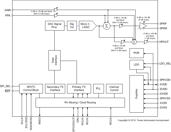
The TAS2505 is a low power digital input speaker amp with support for 24-bit digital I2S data mono playback.
In addition to driving a speaker amp up to 4-Ω, the device also features a mono headphone driver and a programmable digital-signal processing block. The digital audio data format is programmable to work with popular audio standard protocols (I2S, left/right-justified) in master, slave, DSP and TDM modes. The programmable digital-signal processing block can support Bass boost, treble, or EQ functions. An on-chip PLL provides the high-speed clock needed by the digital signal-processing block. The volume level can be controlled by register control. The audio functions are controlled using the I2C serial bus or SPI bus. The device includes an on-board LDO that runs off the speaker power supply to handle all internal device analog and digital power needs. The included POR as power-on-reset circuit reliably resets the device into its default state so no external reset is required at normal usage; however, the device does have a reset pin for more complex system initialization needs. The device also includes two analog inputs for mixing and muxing in both speaker and headphone analog paths.
 Figure 2-1 Simplified Block Diagram
The device can cover operations from 8kHz mono playback to mono 96kHz DAC playback, making it ideal for portable battery-powered audio and telephony applications. The playback path offers signal processing blocks for filtering and effects, flexible mixing of analog input signals as well as programmable volume controls. The voltage supply range for theTAS2505 for analog is 1.5V–1.95V, and for digital it is 1.65V–1.95V. To ease system-level design, a low-dropout regulator (LDO) is integrated to generate the appropriate analog supply from input voltages ranging from 2.7V to 5.5V. Digital I/O voltages are supported in the range of 1.1V–3.6V. The required internal clock of the TAS2505 can be derived from multiple sources, including the MCLK, BCLK or GPIO/DOUT pins or the output of the internal PLL, where the input to the PLL again can be derived from the MCLK, BCLK or GPIO/DOUT pins. Although using the internal, fractional PLL ensures the availability of a suitable clock signal, it is not recommended for the lowest power settings. The PLL is highly programmable and can accept available input clocks in the range of 512kHz to 50MHz.
The device is available in the 4mm × 4mm, 24-pin QFN package.