SLAU873C January 2023 – January 2024
- 1
- Abstract
- Trademarks
- 1Getting Started
-
2Hardware
- 2.1 Jumper Map
- 2.2 Block Diagram
- 2.3
Hardware Features
- 2.3.1 MSPM0G3507 MCU
- 2.3.2 XDS110-ET Onboard Debug Probe With EnergyTrace Technology
- 2.3.3 Debug Probe Connection Isolation Jumper Block
- 2.3.4 Application (or Backchannel) UART
- 2.3.5 Using an External Debug Probe Instead of the Onboard XDS110-ET
- 2.3.6 Using the XDS110-ET Debug Probe With a Different Target
- 2.3.7 Special Features
- 2.4 Power
- 2.5 External Power Supply and BoosterPack Plug-in Module
- 2.6 Measure Current Draw of the MSPM0 MCU
- 2.7 Clocking
- 2.8 BoosterPack Plug-in Module Pinout
- 3Software Examples
- 4Resources
- 5Schematics
- 6Revision History
2.3.7.1 Up to 4-Msps High-Speed Analog-to-Digital Converter
MSPM0 G-series device includes an up to 4-Msps high-speed ADC module. To help evaluate the best performance of the ADC, an external OPA is also included on the LaunchPad kit. This external OPA can be used as a buffer or to amplify the input signal. With the built-in ADC module, the device can achieve a maximum rate of 4 Msps.
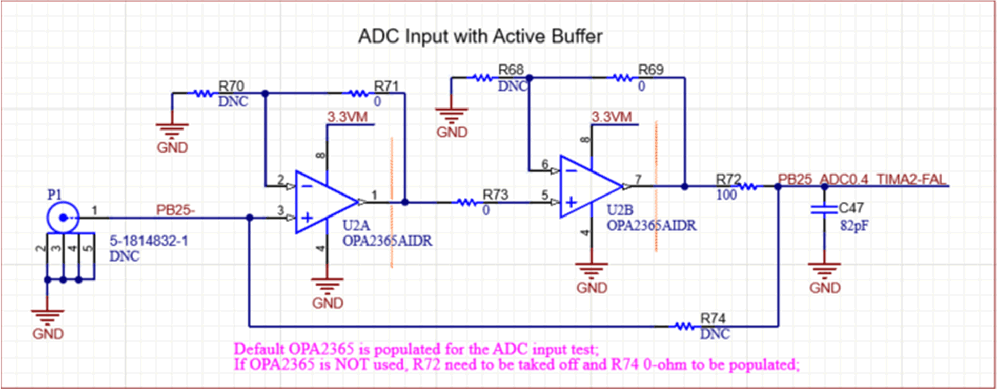
The LaunchPad kit uses the OPA2365 in the ADC input channel in buffer mode by default (see Figure 2-7). The OPA2365 has 2 OPAs inside, and footprints for external passives are provided to allow users to customize the OPA configuration.
 Figure 2-7 External OPA Circuit
For the signal input, a coaxial connector can be populated at P1 to reduce environmental noise. You can also access the OPA input through the pin extension header at the bottom of the board.
The OPA output connects to the ADC0.4 channel, and the example code helps to evaluate ADC performance quickly.