SLAU916 May   2024


  1.   1
  2.   Description
  3.   Getting Started
  4.   Features
  5.   Applications
  6.   6
  7. 1Evaluation Module Overview
    1. 1.1 Introduction
    2. 1.2 Kit Contents
    3. 1.3 Specification
    4. 1.4 Device Information
  8. 2Hardware
    1. 2.1 Hardware Setup
      1. 2.1.1 Hardware Theory of Operation
      2. 2.1.2 Jumper Definitions
      3. 2.1.3 Connector Definitions
      4. 2.1.4 Test Points
    2. 2.2 Hardware Overview
      1. 2.2.1 Connecting the FT4232 Digital Controller
      2. 2.2.2 SPI Configuration
      3. 2.2.3 I2C Configuration
      4. 2.2.4 Glitch Testing
  9. 3Software
    1. 3.1 Software Setup
      1. 3.1.1 Software Installation
    2. 3.2 Software Overview
      1. 3.2.1 Launching the Software
    3. 3.3 Software Features
      1. 3.3.1 Low Level Configuration Page
      2. 3.3.2 High Level Configuration Page
  10. 4Hardware Design Files
    1. 4.1 Schematics
    2. 4.2 PCB Layouts
    3. 4.3 Bill of Materials
  11. 5Additional Information
    1. 5.1 Trademarks
  12. 6Related Documentation

I2C Configuration

Figure 3-4 shows the DAC80516EVM configured for I2C communication.
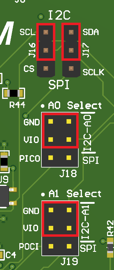
DAC80516EVM DAC80516EVM I2C Configuration Figure 2-4 DAC80516EVM I2C Configuration

The jumper connections on J18 and J19 determine the device address of the DAC80516. The following table shows the required configuration of the A0 and A1 jumpers for specific device addresses.

Table 2-7 I2C Address Configuration
A1A0[A6:A0]
GNDGND101 0000
GNDVIO101 0001
VIOGND101 0100
VIOVIO101 0101