SLLSF21D September 2018 – February 2020
PRODUCTION DATA.
- 1 Features
- 2 Applications
- 3 Description
- 4 Revision History
- 5 Pin Configuration and Functions
-
6 Specifications
- 6.1 Absolute Maximum Ratings
- 6.2 ESD Ratings
- 6.3 Recommended Operating Conditions
- 6.4 Thermal Information
- 6.5 Power Ratings
- 6.6 Insulation Specifications
- 6.7 Safety-Related Certifications
- 6.8 Safety Limiting Values
- 6.9 Electrical Characteristics: Driver
- 6.10 Electrical Characteristics: Receiver
- 6.11 Supply Current Characteristics: Side 1(ICC1)
- 6.12 Supply Current Characteristics: Side 2(ICC2)
- 6.13 Switching Characteristics: Driver
- 6.14 Switching Characteristics: Receiver
- 6.15 Insulation Characteristics Curves
- 6.16 Typical Characteristics
- 7 Parameter Measurement Information
- 8 Detailed Description
- 9 Application and Implementation
- 10Power Supply Recommendations
- 11Layout
- 12Device and Documentation Support
- 13Mechanical, Packaging, and Orderable Information
3 Description
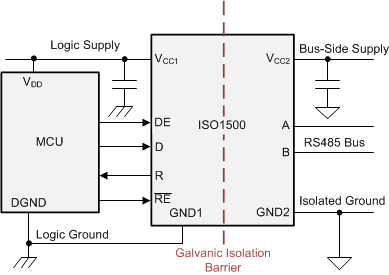
The ISO1500 device is a galvanically-isolated differential line transceiver for TIA/EIA RS-485 and RS-422 applications. This device has a 3-channel digital isolator and an RS-485 transceiver in an ultra-small 16-pin SSOP package. The bus pins of this transceiver are protected against IEC ESD contact discharge and IEC EFT events. The receiver output has a failsafe for bus open, short, and idle conditions. The small solution size of ISO1500 greatly reduces the board space required compared to other integrated isolated RS-485 solutions or discrete implementation with optocouplers and non-isolated RS-485 transceiver.
The device is used for long distance communications. Isolation breaks the ground loop between the communicating nodes, allowing for a much larger common mode voltage range. The symmetrical isolation barrier of each device is tested to provide 3000 VRMS of isolation for 1 minute per UL 1577 between the bus-line transceiver and the logic-level interface.
The ISO1500 device can operate from 1.71 V to 5.5 V on side 1 which lets the devices interface with low-voltage FPGAs and ASICs. The supply voltage on side 2 is from 4.5 V to 5.5 V. This device supports a wide operating ambient temperature range from –40°C to +125°C.
Device Information(1)
| PART NUMBER | PACKAGE | BODY SIZE (NOM) |
|---|---|---|
| ISO1500 | SSOP (16) | 4.90 mm × 3.90 mm |
- For all available packages, see the orderable addendum at the end of the data sheet.
Simplified Schematic
