SLLU368 april 2023
2.2 Operating the THVD24X2VEVM in Default Setup
Out-of-the-box the EVM, when powered, can operate the THVD2452V as a full duplex RS-485 transceiver. The device pins are separated into four distinct groups: single-ended communication pins, differential communication pins, power pins, and control pins. The preceding section Section 2.1 discusses the power pins in depth, the other three types of pins are covered in this section.
The single-ended communication pins are connected directly through the respective jumpers to a single ended bus. These pins are the “R” and “D” pins and represent RX and TX single-ended data, respectively. R is referenced to J6 and D is reference to J16. J6 and J16 are the signal connection points for the EVM.
The EVM board supports two control signals: the enable pins and a slew rate control pin. The enable pins include an active high Driver Enable (DE) pin and an active low Receiver Enable (/RE) pin. These pins are accessed through jumpers J11 and J12, respectively. The Slew Rate Limiting pin (SLR) is a binary input that can implement slew rate limiting to reduce emissions from the device at the cost of lower data rates. The SLR pin is accessed through jumper J20.
The final group of signals, differential bus pins, are pins A, B, Y, and Z. The A and B pins are differential receiver pins that are connected to terminal block J10. As is shown in Figure 2-1, with the board oriented to have J6 at the top-left corner, the 2nd and 3rd pins of J10 are A and B, respectively. Y and Z are the differential driver pins that are connected to terminal block J13. Using the same orientation shown in Figure 2-1, the 2nd and 3rd pins of J13 are differential driver pins Z and Y, respectively.
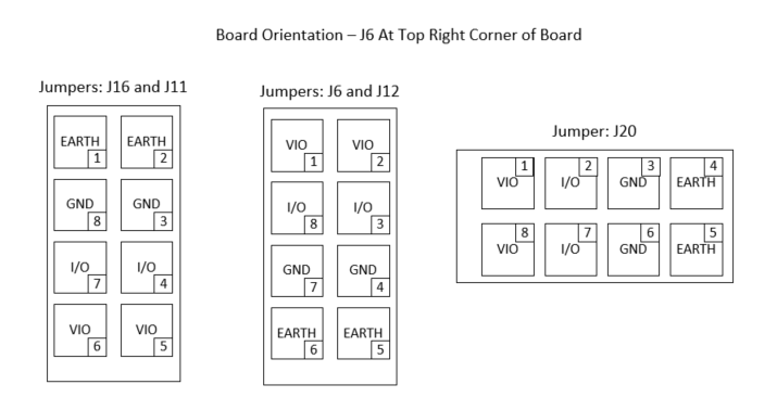
Most signal inputs are use 2x4 headers. Each jumper has a specific mapping that connects the I/O, GND, VIO, and EARTH (when present).
 Figure 2-1 Jumper Map
| Jumper Name | Signal – Jumper Pin | Comment |
|---|---|---|
| J6 | R – J6 Pin 3 or 8 | Receive Data – to keep constant high or low, shunt J6 I/O pins to VIO or GND |
| J11 | /RE – J11 Pin 4 or 7 | /RE – shunt J11 I/O pins to VIO or GND if only one mode is used |
| J12 | DE – J12 Pin 3 or 8 | DE – shunt J12 I/O pins to VIO or GND if only one mode is used |
| J16 | D – J16 Pin 4 or 7 | D – to keep constant high or low, shunt J16 I/O pins to VCC or GND |
| J20 | SLR – Pin 2 or 7 | Shunt I/O pin on J20 to either High (SLR active) or Low (SLR disabled) |
| J10 | Pin 2: A; Pin 3: B | Differential bus input terminal |
| J13 | Pin 2: Z; Pin 3: Y | Differential bus output terminal |
| J1 | N/A | Leave floating for single supply applications, attach digital supply if dual operation is used |
| J2 | N/A | Attach VCC to J2 |
| J7 | N/A | Shunt for single supply Open for dual supply |