SLLU376 December 2023
2.3 Default Operational Mode
With an understanding of how the board is setup and how to power the board, the next topic is how to operate the board. Out of the box the board, when powered, can operate the THVD2412 as a Full Duplex RS-485 transceiver. The devices pins can be broken down into four distinct groups: single ended communication pins, differential communication pins, power pins, and control pins. With the power pins already discussed, the other three categories are now covered.
The single ended communication pins are to be connected directly, through their respective jumpers, to a single ended bus – these pins are the “R” and “D” pins and represent RX and TX single ended data lines respectively. R is referenced to J1 and D is reference to J4; these are the signal connection points for the EVM.
The control signals that this board supports are an active high driver enable (DE) and an active low receiver enable (/RE). These pins follow TTL logic with 0 V to 0.8V for a logic low value and 2 V to VCC for a logic high value. The pins are accessed through Jumpers J3 and J2 respectively
Finally, the last group of signals are the differential bus pins A, B, Y, and Z. The A and B pins are the differential receiver and are connected to a 3-pin terminal block labeled J11 with additional access to the A and B lines through two 4-pin headers J9 and J10. The Y and Z pins are the differential driver pins and are connected to a 3-pin terminal block labeled J14 with additional access to the Y and Z lines through two 4-pin headers J12 and J13. Both differential lines have 0805 component pads for termination capacitances and resistances.
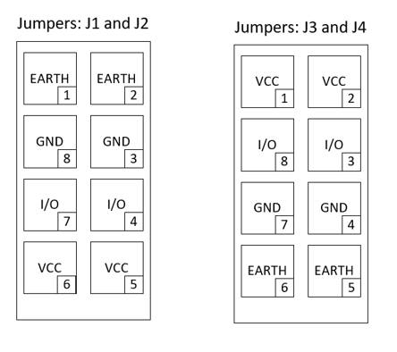
A single ended jumper configuration map can be used to help operate the board. Pin 1 of the header is the top left corner, with J5 at the top of the board, of the shown jumpers with every subsequent pin increasing by one in a clockwise direction.
 Figure 2-1 Single Ended (Console Side)
Jumper Map
Figure 2-1 Single Ended (Console Side)
Jumper Map| Jumper ID | Signal – Jumper Pin | Comment |
|---|---|---|
| J1 | R –Pin 4 or 7 | Receive Data – to keep always high or low shunt J1 I/O pins to VCC or GND. |
| J2 | /RE – Pin 4 or 7 | /RE - shunt J2 I/O pins to VCC or GND to set a constant state on pin. |
| J3 | DE – Pin 3 or 8 | DE– shunt J3 I/O pins to VCC or GND to set a constant state on pin. |
| J4 | D – Pin 3 or 8 | Transmit Data – to keep always high or low shunt J4 I/O pins to VCC or GND |
| J11 | Differential bus input | A and B differential input data |
| J14 | Differential bus output | Y and Z differential output data |