SLOS743M August 2011 – March 2020
PRODUCTION DATA.
- 1Device Overview
- 2Revision History
- 3Device Characteristics
- 4Terminal Configuration and Functions
- 5Specifications
-
6Detailed Description
- 6.1 Overview
- 6.2 System Block Diagram
- 6.3 Power Supplies
- 6.4 Receiver – Analog Section
- 6.5 Receiver – Digital Section
- 6.6 Oscillator Section
- 6.7 Transmitter – Analog Section
- 6.8 Transmitter – Digital Section
- 6.9 Transmitter – External Power Amplifier and Subcarrier Detector
- 6.10 TRF7970A IC Communication Interface
- 6.11 TRF7970A Initialization
- 6.12 Special Direct Mode for Improved MIFARE Compatibility
- 6.13 NFC Modes
- 6.14
Direct Commands from MCU to Reader
- 6.14.1
Command Codes
- 6.14.1.1 Idle (0x00)
- 6.14.1.2 Software Initialization (0x03)
- 6.14.1.3 Initial RF Collision Avoidance (0x04)
- 6.14.1.4 Response RF Collision Avoidance (0x05)
- 6.14.1.5 Response RF Collision Avoidance (0x06, n = 0)
- 6.14.1.6 Reset FIFO (0x0F)
- 6.14.1.7 Transmission With CRC (0x11)
- 6.14.1.8 Transmission Without CRC (0x10)
- 6.14.1.9 Delayed Transmission With CRC (0x13)
- 6.14.1.10 Delayed Transmission Without CRC (0x12)
- 6.14.1.11 Transmit Next Time Slot (0x14)
- 6.14.1.12 Block Receiver (0x16)
- 6.14.1.13 Enable Receiver (0x17)
- 6.14.1.14 Test Internal RF (RSSI at RX Input With TX ON) (0x18)
- 6.14.1.15 Test External RF (RSSI at RX Input with TX OFF) (0x19)
- 6.14.1
Command Codes
- 6.15
Register Description
- 6.15.1 Register Preset
- 6.15.2 Register Overview
- 6.15.3
Detailed Register Description
- 6.15.3.1 Main Configuration Registers
- 6.15.3.2
Control Registers – Sublevel Configuration Registers
- 6.15.3.2.1 ISO/IEC 14443 TX Options Register (0x02)
- 6.15.3.2.2 ISO/IEC 14443 High-Bit-Rate and Parity Options Register (0x03)
- 6.15.3.2.3 TX Timer High Byte Control Register (0x04)
- 6.15.3.2.4 TX Timer Low Byte Control Register (0x05)
- 6.15.3.2.5 TX Pulse Length Control Register (0x06)
- 6.15.3.2.6 RX No Response Wait Time Register (0x07)
- 6.15.3.2.7 RX Wait Time Register (0x08)
- 6.15.3.2.8 Modulator and SYS_CLK Control Register (0x09)
- 6.15.3.2.9 RX Special Setting Register (0x0A)
- 6.15.3.2.10 Regulator and I/O Control Register (0x0B)
- 6.15.3.3
Status Registers
- 6.15.3.3.1 IRQ Status Register (0x0C)
- 6.15.3.3.2 Interrupt Mask Register (0x0D) and Collision Position Register (0x0E)
- 6.15.3.3.3 RSSI Levels and Oscillator Status Register (0x0F)
- 6.15.3.3.4 Special Functions Register (0x10)
- 6.15.3.3.5 Special Functions Register (0x11)
- 6.15.3.3.6 Adjustable FIFO IRQ Levels Register (0x14)
- 6.15.3.3.7 NFC Low Field Level Register (0x16)
- 6.15.3.3.8 NFCID1 Number Register (0x17)
- 6.15.3.3.9 NFC Target Detection Level Register (0x18)
- 6.15.3.3.10 NFC Target Protocol Register (0x19)
- 6.15.3.4 Test Registers
- 6.15.3.5 FIFO Control Registers
- 7Applications, Implementation, and Layout
- 8Device and Documentation Support
- 9Mechanical, Packaging, and Orderable Information
6.6 Oscillator Section
The 13.56-MHz or 27.12-MHz crystal (or oscillator) is controlled by the Chip Status Control register (0x00) and the EN and EN2 terminals. The oscillator generates the RF frequency for the RF output stage as well as the clock source for the digital section. The buffered clock signal is available at pin 27 (SYS_CLK) for any other external circuits. B4 and B5 inside the Modulation and SYS_CLK register (0x09) can be used to divide the external SYS_CLK signal at pin 27 by 1, 2, or 4.
Typical start-up time from complete power down is in the range of 3.5 ms.
During Power Down Mode 2 (EN = 0, EN2 = 1) the frequency of SYS_CLK is switched to 60 kHz (typical).
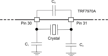
The crystal needs to be connected between pin 30 and pin 31. The external shunt capacitors values for C1 and C2 must be calculated based on the specified load capacitance of the crystal being used. The external shunt capacitors are calculated as two identical capacitors in series plus the stray capacitance of the TRF7970A and parasitic PCB capacitance in parallel to the crystal.
The parasitic capacitance (CS, stray and parasitic PCB capacitance) can be estimated at 4 to 5 pF (typical).
As an example, using a crystal with a required load capacitance (CL) of 18 pF, the calculation is shown in Equation 1.
A 27-pF capacitor must be placed on pins 30 and 31 to ensure proper crystal oscillator operation.
 Figure 6-7 Crystal Block Diagram
 Any crystal used with TRF7970A should meet the minimum characteristics in Table 6-9.
Table 6-9 Minimum Crystal Recommendations
| PARAMETER | SPECIFICATION |
|---|---|
| Frequency | 13.56 MHz or 27.12 MHz |
| Mode of operation | Fundamental |
| Type of resonance | Parallel |
| Frequency tolerance | ±20 ppm |
| Aging | < 5 ppm/year |
| Operation temperature range | –40°C to 85°C |
As an alternative, an external clock oscillator source can be connected to pin 31 to provide the system clock; pin 30 can be left open.