SLUAAC9 March 2021 TPSM5D1806
4 Impact of Current Limits
Every practical voltage regulator requires current limits to protect its components such as power MOSFETs, inductor, and wiring, which all have inherent maximum current ratings (5).
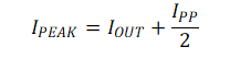
To the first order, inductor ripple, IPP, and peak inductor or HS FET current, IPEAK, are given by Equation 5 and Equation 6. A HS overcurrent limit typically acts to shut off the buck HS FET when the sensed FET or inductor current hits the current limit value.
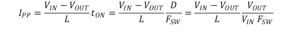
Given a HS overcurrent limit, IHS,OC, the maximum allowed load current is given by Equation 7. In a buck power module where the inductor is fixed, the free variables that influence ripple current are input voltage, output voltage, and switching frequency. For duty cycles below 50%, increasing VOUT or increasing VIN will increase IPP and reduce the maximum allowed load current before hitting the current limit. Operating at a higher switching frequency may be the only means to reduce inductor ripple current to lower the peak current for a fixed input and output voltage requirement.

The TPSM5D1806 is a dual 6-A output power module which uses integrated 470-nH inductors. Figure 4-1 plots the maximum load current versus output voltage for the four selectable frequency settings of the device assuming an input voltage of 12 V and nominal 470-nH inductor. In a real device, there is a delay from the instant the overcurrent threshold is reached to the time the HS FET is actually turned off, which increases the effective current limit and maximum load current allowed. This delay is factored into the maximum load current curves. In addition, the load current curves are clamped to the maximum specified current of 6 A per channel.
")
Figure 4-1 Ideal Maximum Load Current Due to HS Current Limit Only (VIN = 12 V, L = 470 nH)
There are additional factors that impact maximum load current due to current limits. Real inductors will have a tolerance around their nominal inductance values, as well as saturation effects that reduce the effective inductance with applied current. Reducing the 470-nH nominal value by 30% to 325 nH to account for these non-idealities results in higher ripple currents and lowers the maximum load current as shown in Figure 4-2. In addition, considering the tolerance on the internal oscillator, the switching frequency may be lower by 10% which further increases the ripple current and lowers the maximum load current as shown in Figure 4-3.
)")
Figure 4-2 Maximum Load Current Due to HS Current Limit Only (VIN = 12 V, L = 325 nH (70% of Nominal))
")
Figure 4-3 Maximum Load Current Due to HS Current Limit Only (VIN = 12 V, L = 325 nH, -10% FSW)
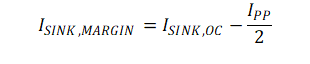
Most modern synchronous buck converters and modules also have a negative current limit or sinking current limit, ISINK,OC. Under no load conditions, the inductor valley current will go negative for devices such as the TPSM5D1806 that operate in forced continuous-conduction mode (FCCM). If too low a switching frequency is used, the steady state inductor current ripple at no load could be large enough that the valley current could exceed the sinking current limit. Thus, a minimum switching frequency is imposed by the sinking current limit. The margin from the sinking current limit is given by Equation 8 and plotted in Figure 4-4 for VIN = 12 V. For a target output voltage, the switching frequency must be selected where there is positive margin from the sinking current limit.
") Figure 4-4 Negative Current Limit Margin
(VIN = 12 V)
Figure 4-4 Negative Current Limit Margin
(VIN = 12 V)The tradeoff of going to higher switching frequency to avoid current limit violations is typically lower efficiency. The TPSM5D1806 data sheet shows the efficiency curves for 12-V input and 1.8-V output at multiple switching frequencies. The 1.8-V efficiency curves for 1 MHz and 1.5 MHz differ at load currents below 3 A, with the 1.5-MHz curve showing lower efficiency owing to higher switching or AC losses than at 1-MHz.
") Figure 4-5 TPSM5D1806
Efficiency vs Output Current (VIN = 12 V)
Figure 4-5 TPSM5D1806
Efficiency vs Output Current (VIN = 12 V)