SLUAAC9 March 2021 TPSM5D1806
3 Impact of Minimum On-Time and Minimum Off-Time
Buck regulators have a minimum on-time and minimum off-time (4) that are the result of gate drive circuitry limitations, control and drive circuit delays, and intentional blanking times. For example, for peak current mode devices with HS MOSFET current sensing, there is a surge in current flowing in the HS FET during its turn-on transition to provide the charge for the LS FET body diode reverse recovery. An initial blanking time in the current sense circuit at the FET turn-on ensures a clean representation of the current is used by the control loop and protection circuitry.
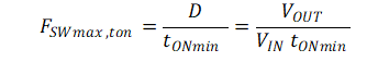
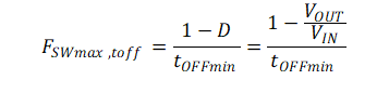
A regulator's minimum on-time and minimum off-time set maximum limits to the allowed switching frequency as defined by Equation 1 and Equation 2 (ignoring resistive voltage drops):
The TPSM5D1806 has a typical minimum on-time, tONmin, of 30 ns and minimum off-time, tOFFmin, of 150 ns. Adding some design margin to typical values is recommended, so values of tONmin of 50 ns and tOFFmin of 200 ns are more conservative numbers used for analysis. Taking an example condition of VIN = 12 V and VOUT = 1 V, the maximum theoretical frequency allowed due to minimum on-time is 1.67 MHz, and maximum theoretical frequency due to minimum off-time is 4.58 MHz. While the minimum off-time is not imposing a limit in this example, the minimum on-time does prohibit the use of the 2-MHz switching frequency option.
When selecting a frequency option for a device with fixed discrete frequency options such as the TPSM5D1806, it is recommended to consider the frequency tolerance as well. The frequency tolerance of the internal oscillator is ±10%, which implies that a device set to 1.5 MHz may have an actual frequency of up to 1.65 MHz, which is close to the 1.67-MHz limit calculated due to min on-time in the previous example. Frequency synchronization to an external clock with tighter accuracy can reduce the required design margins to avoid minimum on- and off-time violations. If the input supply has a wide tolerance or is not well regulated, the maximum and minimum input voltages should be considered when analyzing the maximum allowed frequencies due to minimum on-time and off-time, respectively.
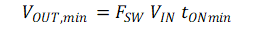
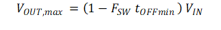
The maximum frequency equations can also be rearranged as Equation 3 and Equation 4 to define the minimum output voltage allowed due to minimum on-time and the maximum output voltage due to minimum off-time at a given frequency and input voltage. The output voltage range due to timing limitations can then be plotted as shown in Figure 3-1 for the TPSM5D1806 at an input voltage of 12 V. The min and max are clamped to the specified output voltage range of the device of 0.5 V to 5.5 V. This figure then makes it easy to read the output voltage range at a given frequency; for example, at 1-MHz switching frequency, the theoretical output voltage range considering only minimum on- and off-times and the basic voltage range limits is 0.7 V to 5.5 V.
")
Figure 3-1 TPSM5D1806 Output Voltage Range Due to Minimum On- and Off-Time Only (VIN = 12 V)