SLUAAR2 august 2023 BQ27Z746
2 Reverse Charger Protection with Optional RCP Circuit
A typical implementation of a reverse charge protection circuit is shown in Figure 2-1. The gate of discharge FET (DFET) is pulled to the source by a high value resistor between the gate and source to ensure it is turned off if the gate drive is open. The resistor value is 10 MΩ in the BQ27Z746 EVM schematic which is described in Figure 1-1. The 10 MΩ resistor ensures that the discharge FET is off in the event of an open connection to the FET driver. The RCP FET, which is an N-channel enhancement MOSFET, is added across RGS (10 MΩ) of the discharge FET with the gate connected to ground as RCP circuit. To use the simple ground gate circuit, the RCP FET must have a low gate turn-on threshold. If it is desired to use a more standard device, such as the 2N7002 as the reference schematic, the gate needs to be biased up to 3.3 V with a high value resistor.
 Figure 2-1 Reverse Cgarge Protection Circuit
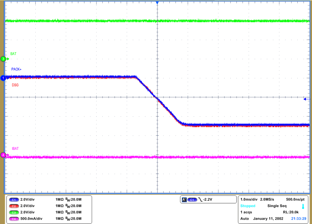
When PACK+ is pulled below VSS, the source of RCP FET is pulled below its gate turning on the FET. Once RCP FET is turned on, it pulls the gate of discharge FET to its source keeping it off, thus preventing current flow. Figure 2-2 shows the waveform once RCP is properly occurred with optional RCP circuit. With the negative voltage on PACK+, the discharge FET sees the sum of the battery and charger voltages. So it must be able to withstand the battery voltage plus the reversed charger voltage considering a suitable VDS voltage. In most cases, this will be at least twice the maximum battery voltage. Any component placed across the discharge FET needs to have a similar rating. The circuit works while the battery and reverse voltages are within the absolute maximum VGS limit of the RCP FET.
 Figure 2-2 Negative Pack+ With optional RCP Circuit