SLUS525A March 2007 – September 2015 TPS61050 , TPS61052
PRODUCTION DATA.
- 1 Features
- 2 Applications
- 3 Description
- 4 Revision History
- 5 Pin Configuration and Functions
- 6 Specifications
- 7 Detailed Description
-
8 Application and Implementation
- 8.1 Application Information
- 8.2
Typical Applications
- 8.2.1 Typical Application Schematic
- 8.2.2 High-Power White LED Solution Featuring Privacy Indicator
- 8.2.3 High-Power White LED Solution Featuring No-Latency Turn-Down Through PA TX Signal
- 8.2.4 High-Power White LED Flash Driver And AF/Zoom Motor Drive Supply
- 8.2.5 White LED Flash Driver and Audio Amplifier Power Supply Exclusive Operation
- 8.2.6 White LED Flash Driver and Audio Amplifier Power Supply Operating Simultaneously
- 8.2.7 White LED Flash Driver and Auxiliary Lighting Zone Power Supply
- 8.2.8 2 × 300 mA Dual LED Camera Flash
- 9 Power Supply Recommendations
- 10Layout
- 11Device and Documentation Support
- 12Mechanical, Packaging, and Orderable Information
8 Application and Implementation
NOTE
Information in the following applications sections is not part of the TI component specification, and TI does not warrant its accuracy or completeness. TI’s customers are responsible for determining suitability of components for their purposes. Customers should validate and test their design implementation to confirm system functionality.
8.1 Application Information
The TPS6105x device is based on a high-frequency synchronous-boost topology with constant current sink to drive single white LEDs. The TPS6105x device not only operates as a regulated current source but also as a standard voltage-boost regulator. This additional operating mode can be useful to supply other high-power devices in the system, such as a hands-free audio power amplifier, or any other component requiring a supply voltage higher than the battery voltage.
8.2 Typical Applications
8.2.1 Typical Application Schematic
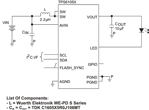 Figure 40. Typical Application Schematic
8.2.1.1 Design Requirements
This example illustrates how to use the TPS6105x to drive high power white LED. Table 3 shows the design parameters and example values.
Table 3. Design Parameters
| DESIGN PARAMETERS | EXAMPLE VALUES |
|---|---|
| Input voltage range | 3.3 V to 4.2 V |
| Output voltage | 5 V |
| Flash current | 500 mA |
8.2.1.2 Detailed Design Procedure
8.2.1.2.1 Inductor Selecton
A boost converter requires two main passive components for storing energy during the conversion. A boost inductor and a storage capacitor at the output are required. The TPS6105x device integrates a current limit protection circuitry. The peak current of the NMOS switch is sensed to limit the maximum current flowing through the switch and the inductor. The typical peak current limit (1000 mA / 1500 mA / 2000 mA) is user selectable through the I2C interface.
To optimize solution size the TPS6105x device has been designed to operate with inductance values from a minimum of 1.3 μH to a maximum of 2.9 μH. In typical high-current white LED applications, TI recommends an inductance of 2.2 μH.
To select the boost inductor, TI recommends keeping the possible peak inductor current below the current limit threshold of the power switch in the chosen configuration. The highest peak current through the inductor and the power switch depends on the output load, the input and output voltages. Estimation of the maximum average inductor current and the maximum inductor peak current can be done using Equation 1 and Equation 2:


with:
f = switching frequency (2 MHz)
L = inductance value (2.2 μH)
η = estimated efficiency (85%)
For example, for an output current of 500 mA at 5 V, the TPS6105x device must be set for a 1000 mA current limit operation together with an inductor supporting this peak current.
The losses in the inductor caused by magnetic hysteresis losses and copper losses are a major parameter for total circuit efficiency.
Table 4. List of Inductors
| MANUFACTURER | SERIES | DIMENSIONS | ILIM SETTINGS |
|---|---|---|---|
| TDK | VLF3010AT | 2.6 mm × 2.8 mm × 1 mm maximum height | 1000 mA (typical) |
| TAIYO YUDEN | NR3010 | 3 mm × 3 mm × 1 mm maximum height | |
| TDK | VLF3014AT | 2.6 mm × 2.8 mm × 1.4 mm maximum height | 1500 mA (typical) |
| COILCRAFT | LPS3015 | 3 mm × 3 mm × 1.5 mm maximum height | |
| MURATA | LQH3NP | 3 mm × 3 mm × 1.5 mm maximum height | |
| TOKO | FDSE0312 | 3 mm × 3 mm × 1.2 mm maximum height | 2000 mA (typical) |
8.2.1.2.2 Capacitor Selection
8.2.1.2.2.1 Input Capacitor
For good input voltage filtering low ESR ceramic capacitors are recommended. A 10-μF input capacitor is recommended to improve transient behavior of the regulator and EMI behavior of the total power supply circuit. The input capacitor should be placed as close as possible to the input pin of the converter.
8.2.1.2.2.2 Output Capacitor
The primary parameter necessary to define the output capacitor is the maximum allowed output voltage ripple of the converter. This ripple is determined by two parameters of the capacitor, the capacitance and the ESR. It is possible to calculate the minimum capacitance needed for the defined ripple, supposing that the ESR is zero, by using Equation 3:

Parameter f is the switching frequency and ΔV is the maximum allowed ripple.
With a chosen ripple voltage of 10mV, a minimum capacitance of 10 μF is needed. The total ripple is larger due to the ESR of the output capacitor. This additional component of the ripple can be calculated using Equation 4:
The total ripple is the sum of the ripple caused by the capacitance and the ripple caused by the ESR of the capacitor. Additional ripple is caused by load transients. This means that the output capacitor must completely supply the load during the charging phase of the inductor. A reasonable value of the output capacitance depends on the speed of the load transients and the load current during the load change.
For the high current white LED application, a minimum of 3-μF effective output capacitance is usually required when operating with 2.2-μH (typical) inductors. For solution size reasons, this is usually one or more X5R/X7R ceramic capacitors. For stable operation of the internally compensated control loop, a maximum of 50 μF effective output capacitance is tolerable.
Depending on the material, size and margin to the rated voltage of the used output capacitor, degradation on the effective capacitance can be observed. This loss of capacitance is related to the DC bias voltage applied. It is therefore always recommended to check that the selected capacitors are showing enough effective capacitance under real operating conditions.
8.2.1.2.3 Checking Loop Stability
The first step of circuit and stability evaluation is to look from a steady-state perspective at the following signals:
- Switching node, SW
- Inductor current, IL
- Output ripple voltage, VOUT(AC)
These are the basic signals that must be measured when evaluating a switching converter. When the switching waveform shows large duty cycle jitter or the output voltage or inductor current shows oscillations the regulation loop may be unstable. This is often a result of board layout and/or L-C combination.
The next step in regulation loop evaluation is to perform a load transient test. Output voltage settling time after the load transient event is a good estimate of the control loop bandwidth. The amount of overshoot and subsequent oscillations (ringing) indicates the stability of the control loop. Without any ringing, the loop has usually more than 45° of phase margin.
Because the damping factor of the circuitry is directly related to several resistive parameters (for example, MOSFET rDS(on)) that are temperature dependant, the loop stability analysis must be done over the input voltage range, output current range, and temperature range.
8.2.1.3 Application Curves
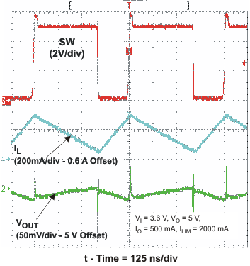 Figure 41. PWM Operation
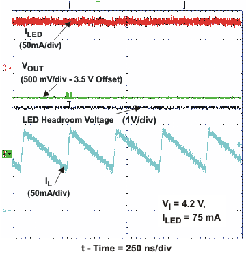 Figure 42. Down-Mode Operation
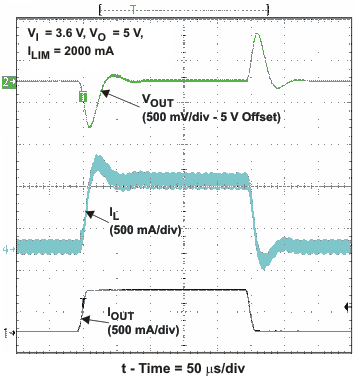 Figure 43. Voltage Mode Load Transient Response
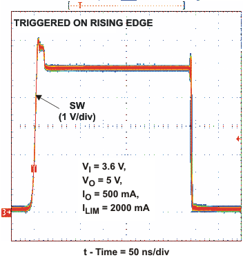 Figure 45. Duty Cycle Jitter
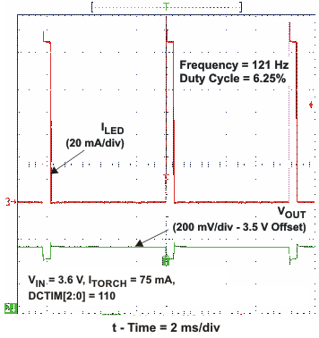 Figure 47. Low-Light Dimming Mode Operation
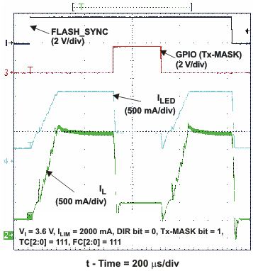 Figure 49. TX-Masking Operation
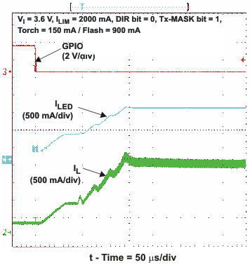 Figure 51. TX-Masking Operation
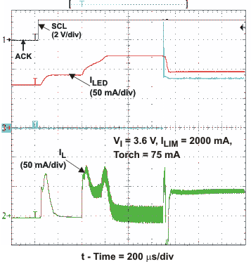 Figure 53. Start-Up in Torch Operation
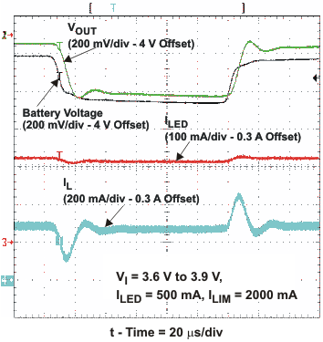 Figure 44. Down-Mode Line Transient Response
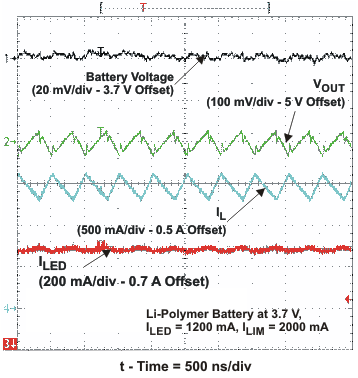 Figure 46. Input Ripple Voltage
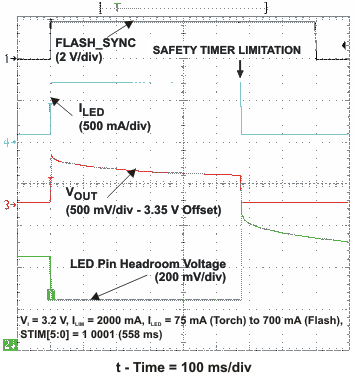 Figure 48. Torch/Flash Sequence
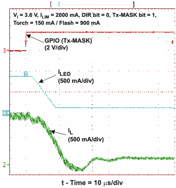 Figure 50. TX-Masking Operation
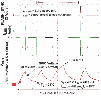 Figure 52. Junction Temperature Monitoring
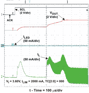 Figure 54. Start-Up in Torch Operation
8.2.2 High-Power White LED Solution Featuring Privacy Indicator
Figure 55 shows the typical application where TPS61050 is used to drive high-power white LED with a privacy indicator feature.
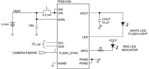 Figure 55. High-Power White LED Solution Featuring Privacy Indicator
8.2.3 High-Power White LED Solution Featuring No-Latency Turn-Down Through PA TX Signal
Figure 56 shows the typical application where TPS61050 is used to drive high-power white LED, and the RF PA TX signal is used to realize the no-latency turn down function.
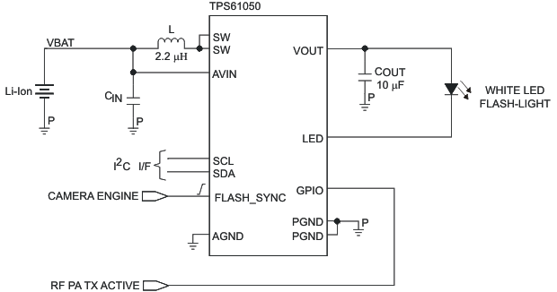 Figure 56. High-Power White LED Solution Featuring No-Latency Turn-Down Through PA TX Signal
8.2.4 High-Power White LED Flash Driver And AF/Zoom Motor Drive Supply
Figure 57 shows the typical application where TPS61052 is used as high-power white LED flash driver and meantime to provide the power supply to the AF/Zoom motor driver.
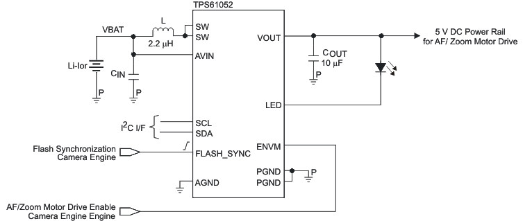 Figure 57. High-Power White LED Flash Driver And AF/Zoom Motor Drive Supply
8.2.5 White LED Flash Driver and Audio Amplifier Power Supply Exclusive Operation
Figure 58 shows the typical application where TPS61052 is used as white LED flash driver and it can also be used to provide the power supply to the audio amplifier exclusively by using a logic gate 1G97.
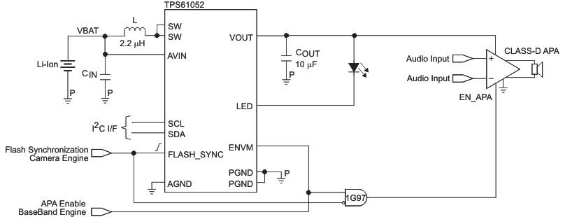 Figure 58. White LED Flash Driver and Audio Amplifier Power Supply Exclusive Operation
8.2.6 White LED Flash Driver and Audio Amplifier Power Supply Operating Simultaneously
Figure 59 shows the typical application where TPS61052 is used as white LED flash driver and meantime to provide the power supply to the audio amplifier simultaneously.
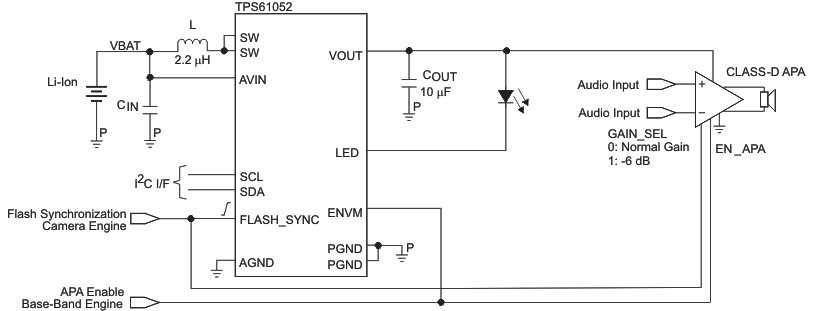 Figure 59. White LED Flash Driver and Audio Amplifier Power Supply Operating Simultaneously
8.2.7 White LED Flash Driver and Auxiliary Lighting Zone Power Supply
Figure 60 shows the typical application where TPS61052 is used as white LED flash driver and meantime to provide the supply to the auxiliary lighting zone (TCA6507 in this example).
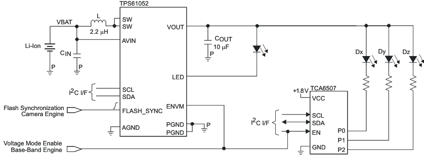 Figure 60. White LED Flash Driver and Auxiliary Lighting Zone Power Supply
8.2.8 2 × 300 mA Dual LED Camera Flash
Figure 61 shows the typical application where TPS61050 is used to drive dual LED camera flash (2 × 300 mA).
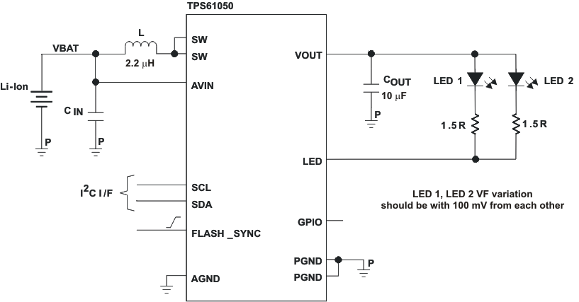 Figure 61. 2 × 300 mA Dual LED Camera Flash