SLUS670C JULY 2005 – January 2015
PRODUCTION DATA.
- 1 Features
- 2 Applications
- 3 Description
- 4 Revision History
- 5 Pin Configuration and Functions
- 6 Specifications
-
7 Detailed Description
- 7.1 Overview
- 7.2 Functional Block Diagram
- 7.3
Feature Description
- 7.3.1 PWM Operation
- 7.3.2 Adaptive On-Time Control
- 7.3.3 Light Load Operation
- 7.3.4 Forced PWM Operation
- 7.3.5 5-V, 100-mA, LDO and Switchover (VREG5)
- 7.3.6 3.3-V, 100-mA, LDO and Switchover (VREG3)
- 7.3.7 2-V, 50-uA Sink - Source Reference (VREF2)
- 7.3.8 Low-Side Driver
- 7.3.9 High-Side Driver
- 7.3.10 Soft-Start
- 7.3.11 Soft-Stop
- 7.3.12 Powergood
- 7.3.13 Current Sensing and Overcurrent Protection
- 7.3.14 Overvoltage Protection
- 7.3.15 Undervoltage Protection
- 7.3.16 5-V Supply and UVLO Protection
- 7.3.17 VIN Line Sag Protection (Dynamic UVP)
- 7.3.18 Thermal Shutdown
- 7.4 Device Functional Modes
- 7.5 Programming
- 8 Application and Implementation
- 9 Power Supply Recommendations
- 10Layout
- 11Device and Documentation Support
- 12Mechanical, Packaging, and Orderable Information
1 Features
- 3.3-V and 5-V 100-mA Bootstrapped Standby Regulators with Independent Enables
- Selectable D-CAP™ Mode Enables Fast Transient Response Less than 100 ns
- Selectable Low Ripple Current Mode
- Less than 1% Internal Reference Accuracy
- Selectable PWM-only/Auto-skip Modes
- Low-side RDS(on) Loss-less Current Sensing
- RSENSE Accurate Current Sense Option
- Internal Soft-Start and Integrated VOUT Discharge Transistors
- Integrated 2-V Reference
- Adaptive Gate Drivers with Integrated Boost Diode
- Powergood for Each Channel with Delay Timer
- Fault Disable Mode
- Supply Input Voltage Range: 4.5 V to 28 V
2 Applications
Notebook Computers System Bus and I/O
3 Description
The TPS51120 is a highly sophisticated dual, synchronous step-down controller. It is a full featured controller designed to run directly off a three- or four-cell Li-ion battery and provide high-power and 5-V and/or 3.3-V standby regulation for all the downstream circuitry in a notebook computer system. High-current, 100-mA, 5-V or 3.3-V on-board linear regulators have glitch-free switch over function to SMPS and can be kept alive independently during standby state. The pseudo-constant frequency adaptive on-time control scheme supports full range of current mode operation including simplified loop compensation, ceramic output capacitors as well as seamless transition to reduced frequency operation at light-load condition. Optional D-CAP mode operation optimized for SP-CAP or POSCAP output capacitors allows further reduction of external compensation parts. Dynamic UVP supports VIN line sag without latch off by hitting 5-V UVP. No negative voltage appears at output voltage node during UVLO, UVP, and OCP, OTP or loss of VIN.
The TPS51120 32-pin QFN package is specified from –40°C to 85°C ambient temperature.
Device Information(1)
| PART NUMBER | PACKAGE | BODY SIZE (NOM) |
|---|---|---|
| TPS51120 | VQFN (32) | 5.00 mm × 5.00 mm |
- For all available packages, see the orderable addendum at the end of the datasheet.
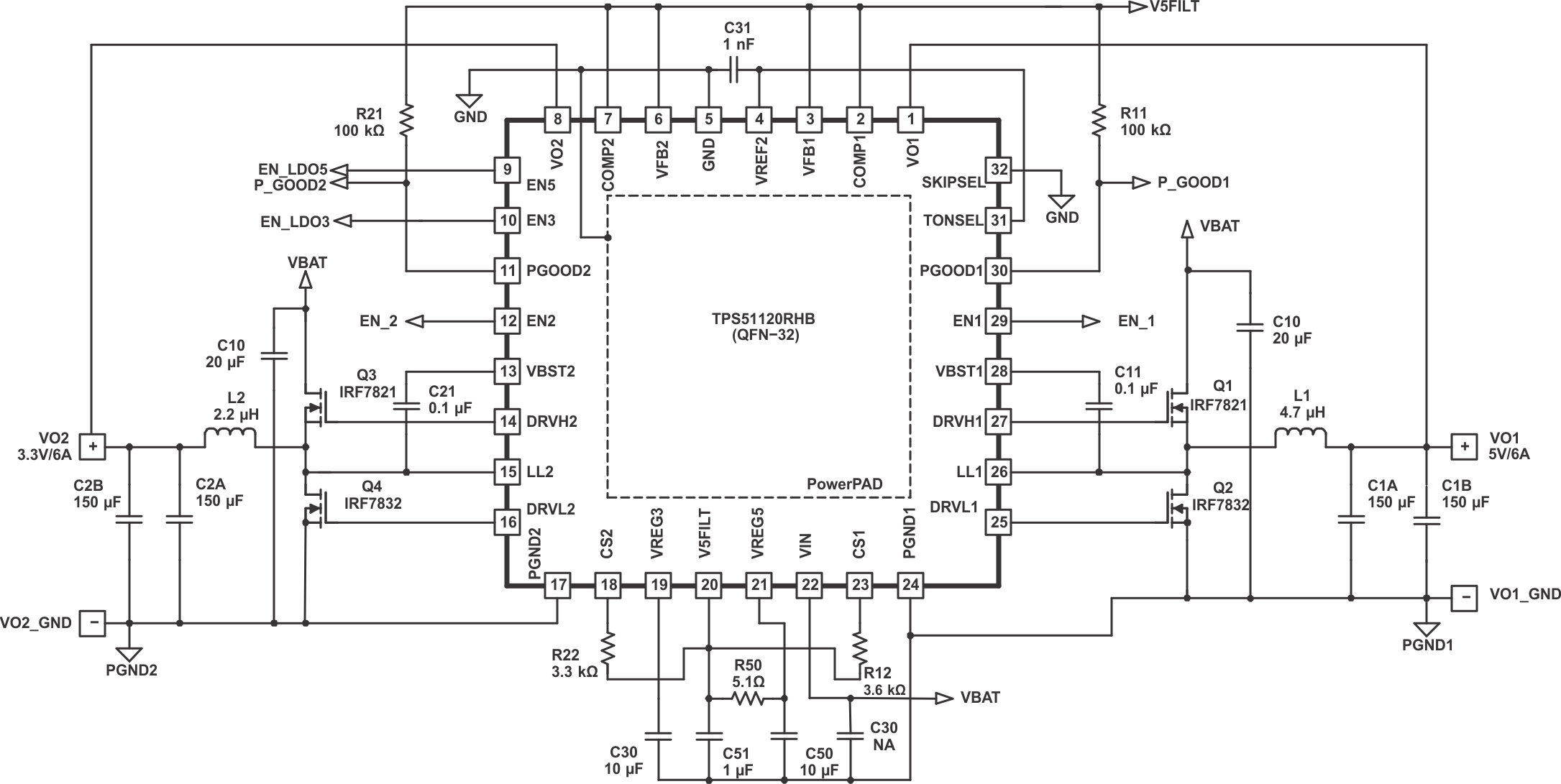
Reference Design for D-CAP Mode Converter
