SLUSAP5A December 2011 – November 2016 TPS53316
PRODUCTION DATA.
- 1 Features
- 2 Applications
- 3 Description
- 4 Revision History
- 5 Pin Configuration and Functions
- 6 Specifications
- 7 Detailed Description
- 8 Application and Implementation
- 9 Power Supply Recommendations
- 10Layout
- 11Device and Documentation Support
- 12Mechanical, Packaging, and Orderable Information
8 Application and Implementation
NOTE
Information in the following applications sections is not part of the TI component specification, and TI does not warrant its accuracy or completeness. TI’s customers are responsible for determining suitability of components for their purposes. Customers should validate and test their design implementation to confirm system functionality.
8.1 Application Information
The TPS53316 device is a high-efficiency synchronous-buck converter. The device suits low output voltage point-of-load applications with 5-A or lower output current in computing and similar digital consumer applications.
8.2 Typical Application
This design example describes a voltage-mode, 5-A synchronous buck converter with integrated MOSFETs. The device provides a fixed 1.5-V output at up to 5 A from a 5-V input bus.
8.2.1 Design Requirements
Table 3 lists the parameters for this design example.
Table 3. TPS53316 Design Example Specifications
| PARAMETER | TEST CONDITIONS | MIN | TYP | MAX | UNIT |
|---|---|---|---|---|---|
| INPUT CHARACTERISTICS | |||||
| Voltage range | VIN | 2.9 | 3.3 or 5 | 6 | V |
| Maximum input current | VIN = 5 V, IOUT = 5 A | 1.76 | A | ||
| No load input current | No load input current VIN = 5 V, IOUT = 0 A under DE/HEF mode |
3 | mA | ||
| OUTPUT CHARACTERISTICS | |||||
| Output voltage | 1.5 | V | |||
| Output voltage regulation | Setpoint accuracy (VIN = 2.9 V – 6 V, IOUT = 0 A – 5 A) |
–1% | 1% | ||
| Line regulation (VIN = 2.9 V – 6 V, IOUT = 5 A) |
0.1% | ||||
| Load regulation (VIN = 5 V, IOUT = 0 A – 5 A) |
0.1% | ||||
| Output voltage ripple | VIN = 5 V, IOUT = 5 A | 10 | mVPP | ||
| Output load current | 0 | 5 | A | ||
| Overcurrent limit | VIN = 3.3V, fSW = 750 kHz | 6.5 or 4.5 | A | ||
| SYSTEM CHARACTERISTICS | |||||
| Switching frequency | 0.75 | MHz | |||
| Peak efficiency | VIN = 5 V, IOUT = 1.8 A, fSW = 750 kHz | 92.7% | |||
| Full-load efficiency | VIN = 5 V, IOUT = 5 A, fSW = 750 kHz | 89% | |||
| Operating temperature | 25 | ºC | |||
8.2.2 Detailed Design Procedure
Select the external components using the following steps.
8.2.2.1 Determine the Value of R1 and R2
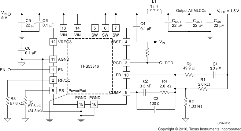
The output voltage is programmed by the voltage-divider resistor, R1 and R2 shown in Figure 38. R1 is connected between VFB pin and the output, and R2 is connected between the VFB pin and GND. Recommended value for R1 is between 1 kΩ and 10 kΩ. Determine R2 using Equation 1.

8.2.2.2 Choose the Inductor
The inductance value must be determined to give the ripple current of approximately 20% to 40% of maximum output current. The inductor ripple current is determined by Equation 2.

The inductor also must have a low DCR to achieve good efficiency, as well as enough room above peak inductor current before saturation.
8.2.2.3 Choose the Output Capacitor(s)
The output capacitor selection is determined by output ripple and transient requirement. When operating in CCM, the output ripple has three components. VRIPPLE(C) represents the ripple due to the output capacitance and is shown in Equation 4.


When ceramic output capacitor is chosen, the ESL component is usually negligible. In the case when multiple output capacitors are used, the total ESR and ESL must be the equivalent of the all output capacitors in parallel.
When operating in DCM, the output ripple is dominated by the component determined by capacitance. It also varies with load current and can be expressed as shown in Equation 7.

where
- α is the DCM on-time coefficient (typical value is 1.25) and can be expressed as

Figure 39 illustrates the DCM output voltage ripple.
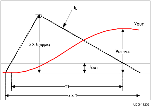 Figure 39. Discontinuous Mode Output Voltage Ripple
8.2.2.4 Choose the Input Capacitors
The selection of input capacitor must be determined by the ripple current requirement. The ripple current generated by the converter must be absorbed by the input capacitors as well as the input source. The RMS ripple current from the converter can be expressed as shown in Equation 8.

where
- D is the duty cycle and can be expressed as

To minimize the ripple current drawn from the input source, sufficient input decoupling capacitors must be placed close to the device. The ceramic capacitor is recommended due to the low ESR and low ESL. The input voltage ripple can be calculated in Equation 9 when the total input capacitance is determined.

8.2.2.5 Compensation Design
The TPS53316 employs voltage mode control. To effectively compensation the power stage and ensures fast transient response, Type III compensation is typically used.
The control to output transfer function can be described in Equation 10.

The output LC filter introduces a double pole which can be calculated in Equation 11.

The ESR zero of can be calculated in Equation 12.

Figure 40 shows the configuration of Type III compensation and typical pole and zero locations. Equation 13 through Equation 15 describe the compensator transfer function and poles and zeros of the Type III network.


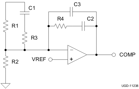 Figure 40. Type III Compensation Network Schematic
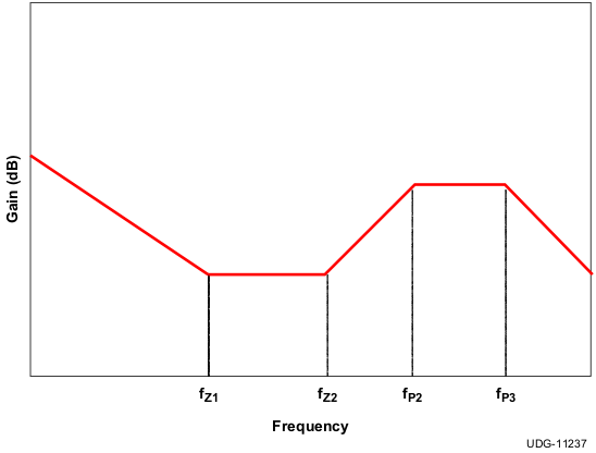 Figure 41. Type III Compensation Network Waveform


The two zeros can be placed near the double-pole frequency to cancel the response from the double pole. One pole can be used to cancel ESR zero, and the other non-zero pole can be placed at half switching frequency to attenuate the high frequency noise and switching ripple. Suitable values can be selected to achieve a compromise between high phase margin and fast response. A phase margin higher than 45° is required for stable operation.
For DCM operation, a C3 capacitor value between 56 pF and 150 pF is recommended for output capacitance between 20 µF to 200 µF.
8.2.3 Application Curves
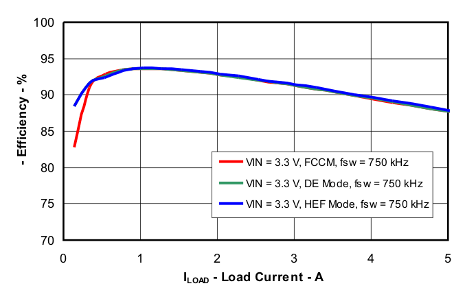 Figure 42. 3.3-V Input Efficiency
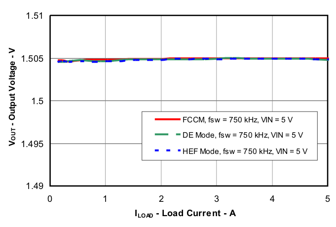
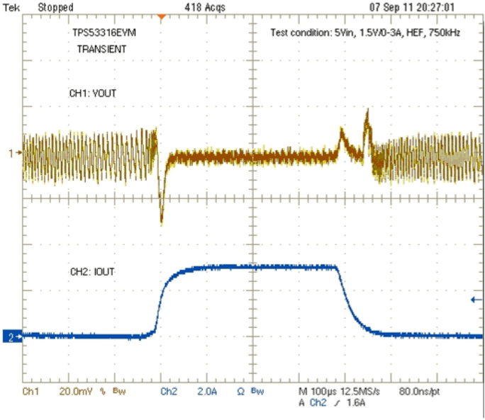
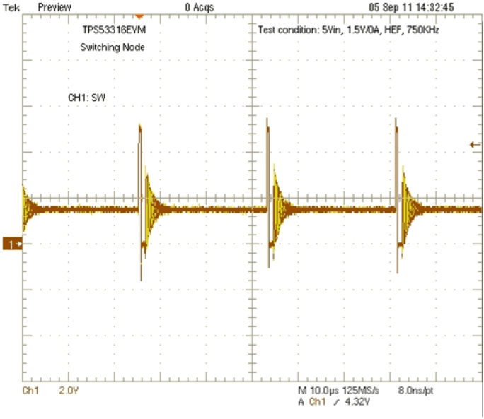
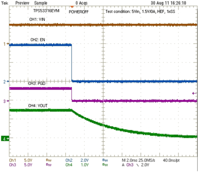
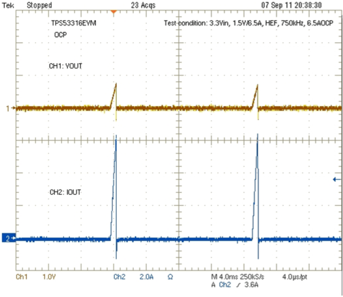
and 6.5-A OCP
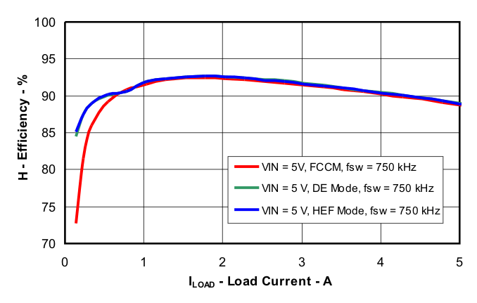 Figure 43. 5-V Input Efficiency
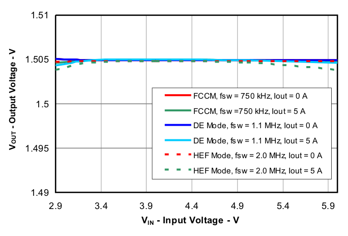
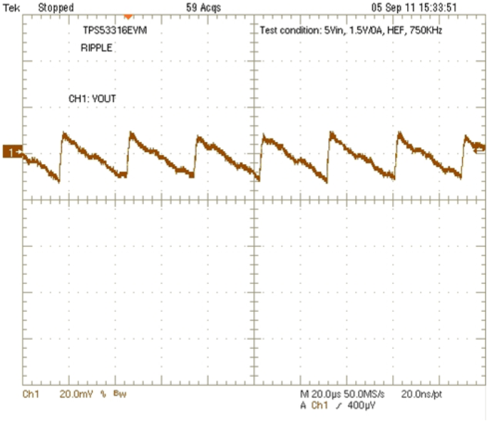
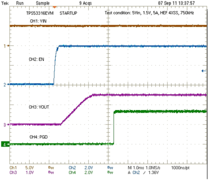
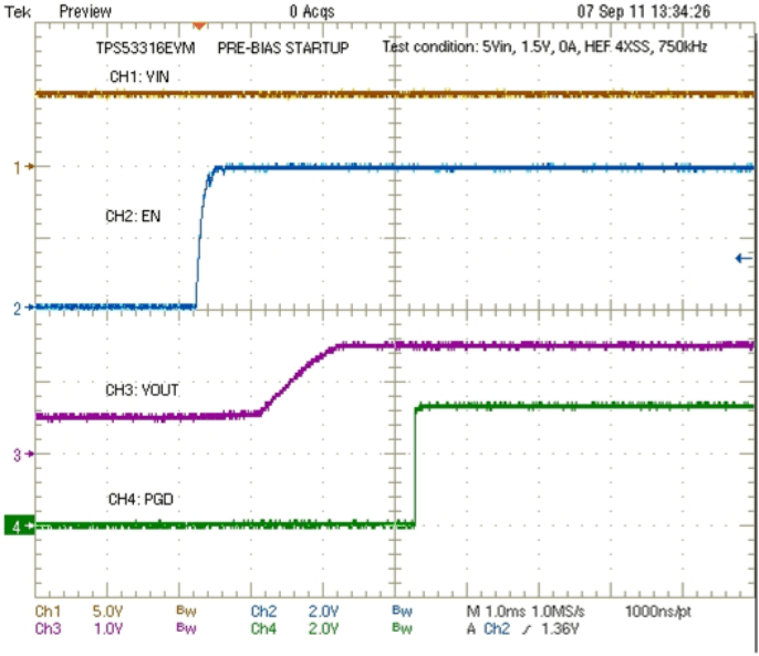
and 0.5-V prebias
