SLUUC79A May 2020 – February 2022 TPS51215A
4 Board Layout
This section provides a description of the TPS51215AEVM board layout and layer illustrations. The board layout for the TPS51215AEVM is shown in Figure 4-1 to Figure 4-9. The top and bottom are 2-oz. copper and internal layers are 1-oz. copper.
VIN capacitors, VOUT capacitors, and MOSFETs are the power components and should be placed on one side of the PCB (solder side). At least one inner plane should be inserted, connected to ground, in order to shield and isolate the small signal traces from noisy power lines.
All sensitive analog traces and components such as VSNS, SLEW, VID, VREF, and TRIP should be placed away from high-voltage switching nodes such as SW, DRVH, DRVL, or BST to avoid coupling. Use internal layer or layers as ground plane or planes and shield feedback trace from power traces and components.
Connect VSNS directly to the output voltage sense point at the load device. Connect GSNS to ground return points at the load device. Routing as differential lines to avoid noise coupling.
Connect the overcurrent setting resistors from the TRIP pin to ground and make the connections as close as possible to the device. The trace from TRIP pin to resistor and from resistor to ground should avoid coupling to a high-voltage switching node.
Connections from gate drivers to the respective gate of the high-side or the low-side MOSFET should be as short as possible to reduce stray inductance.
The PCB trace defined as SW node, which connects to the source of the switching MOSFET, the drain of the rectifying MOSFET and the high-voltage side of the inductor, should be as short and wide as possible.
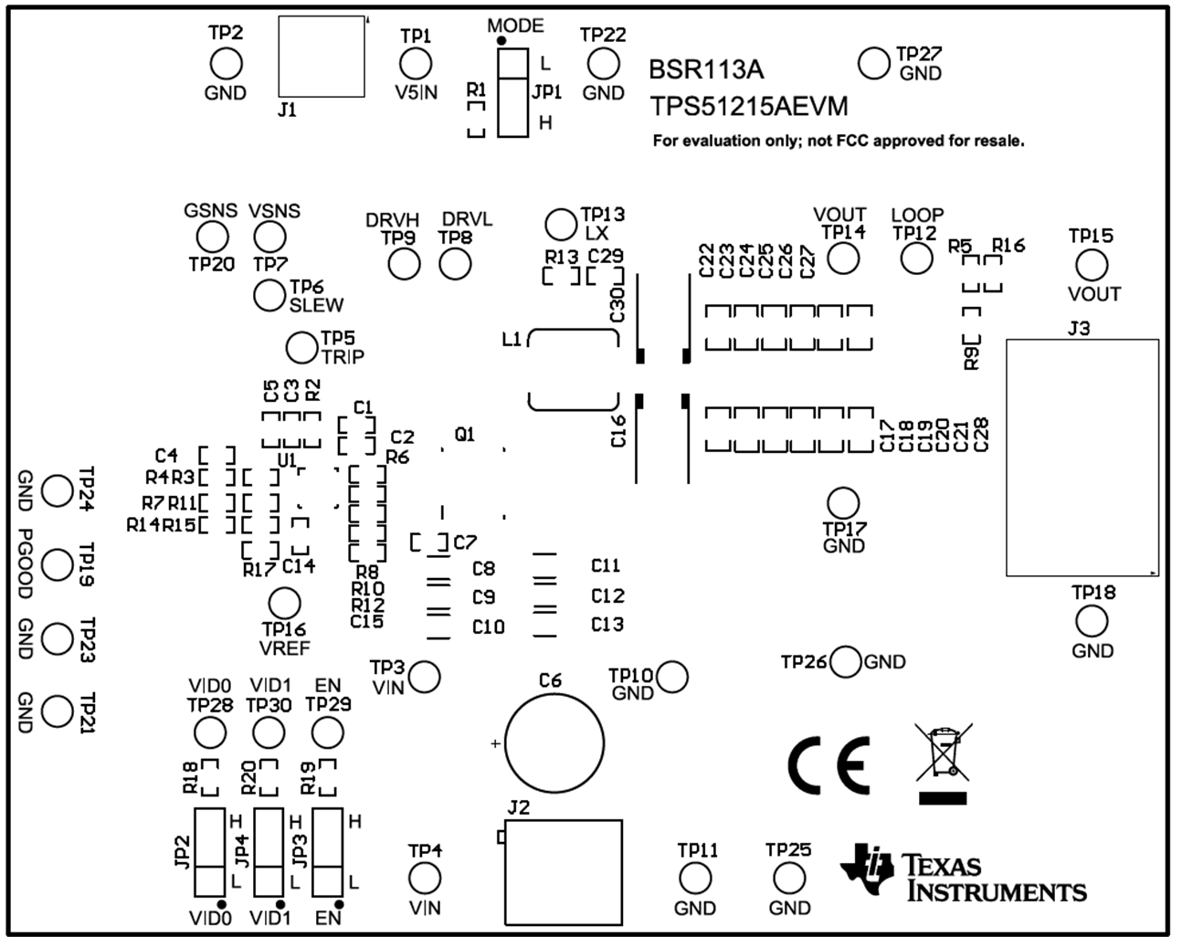 Figure 4-1 Top Assembly
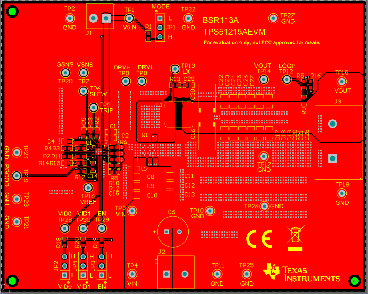 Figure 4-2 Top Layer
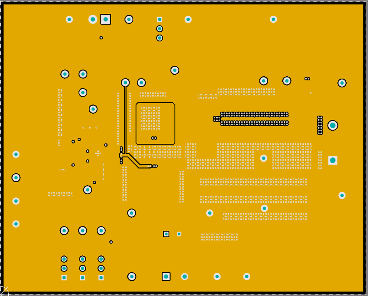 Figure 4-3 Inner1 Layer
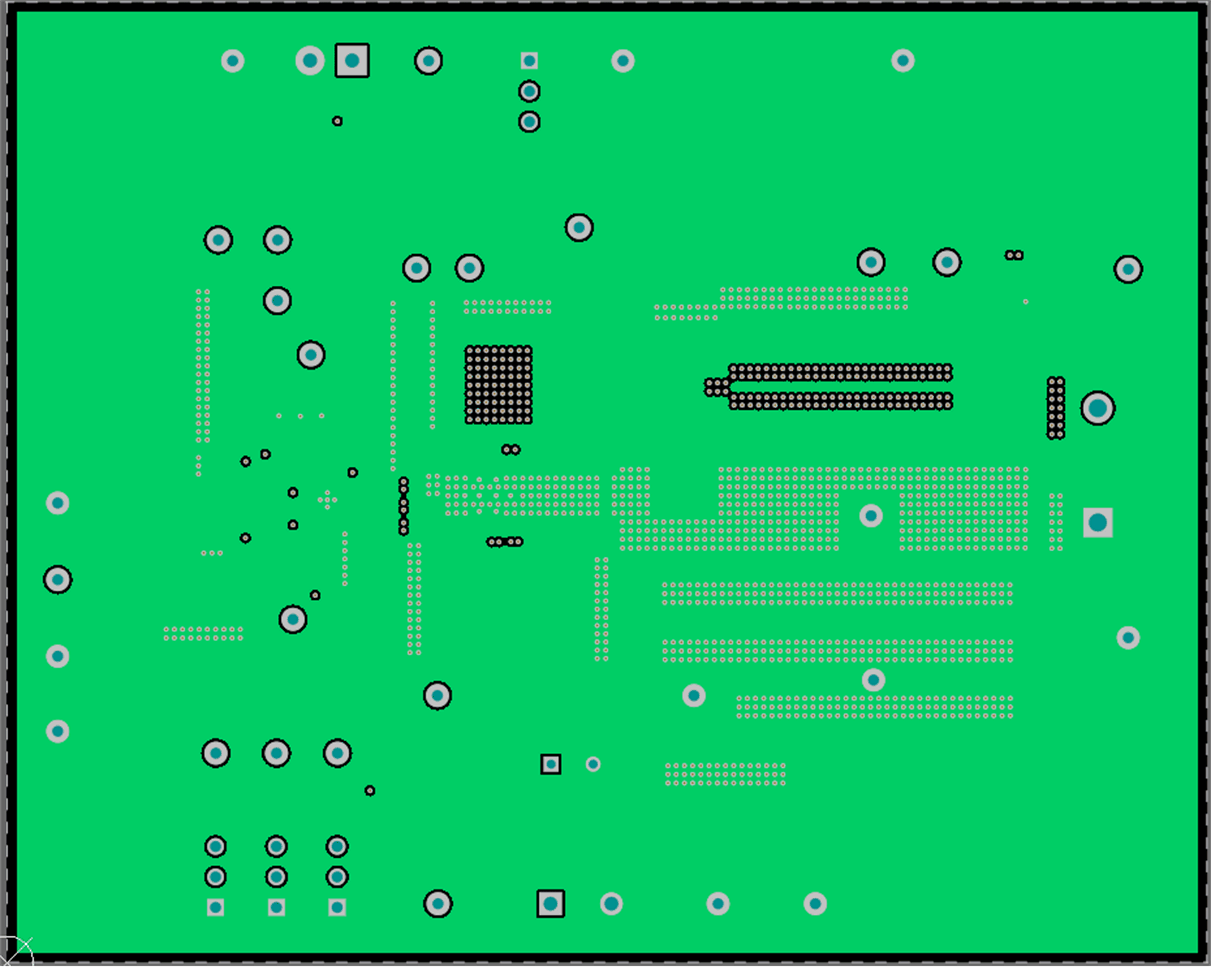 Figure 4-4 Inner2 Layer
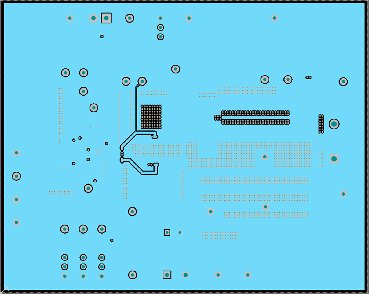 Figure 4-5 Inner3 Layer
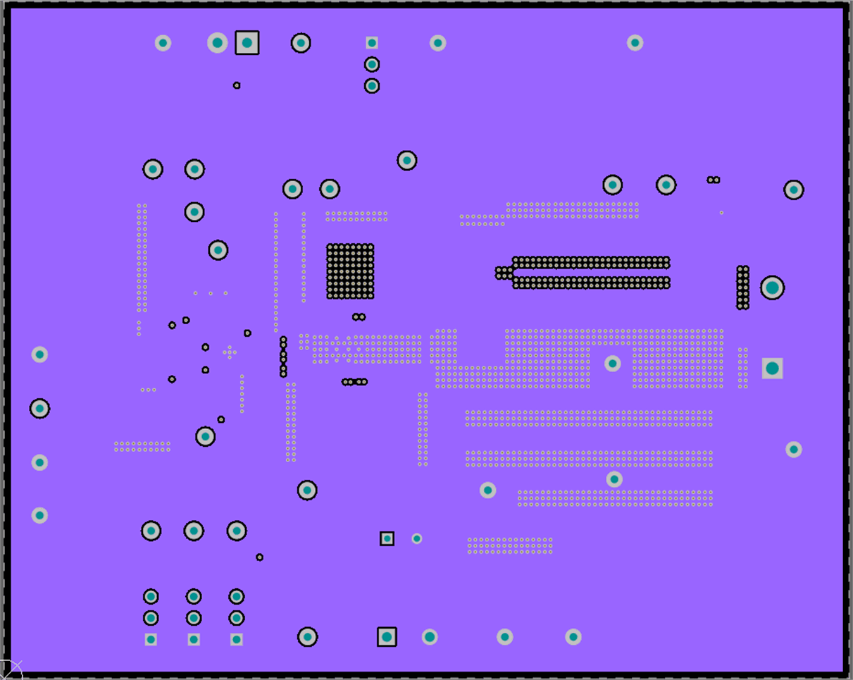 Figure 4-6 Inner4 Layer
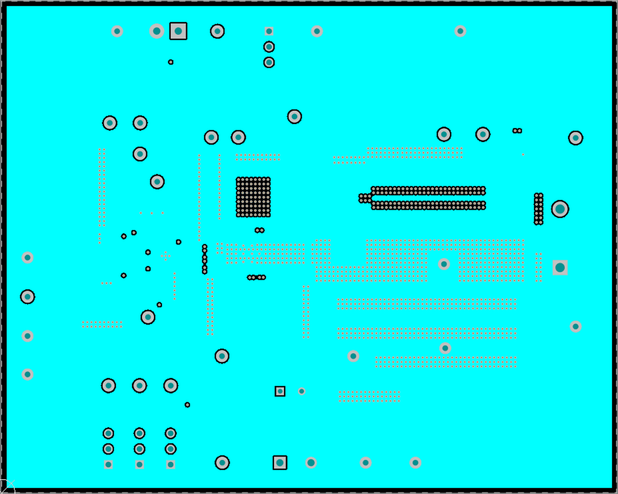 Figure 4-7 Inner5 Layer
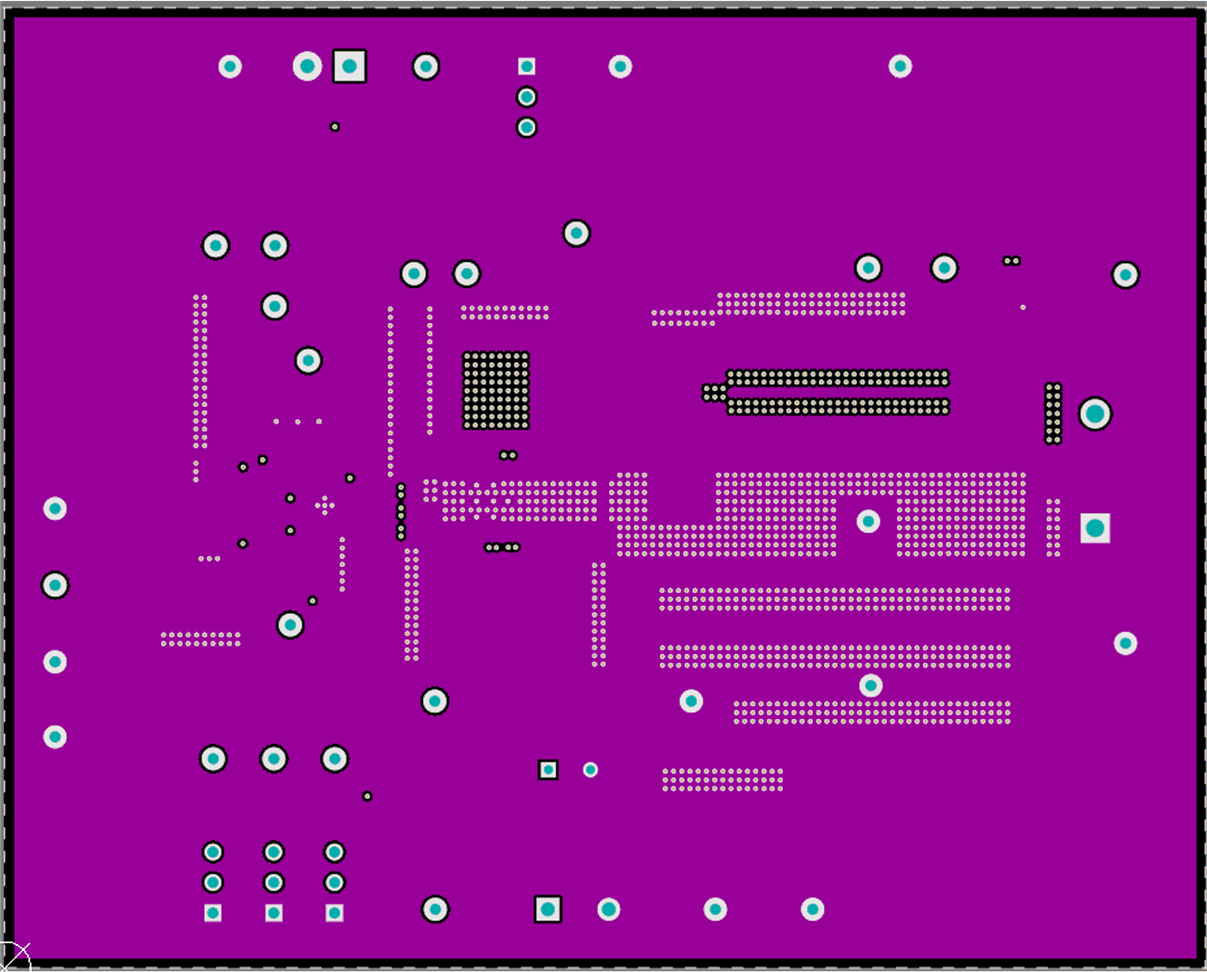 Figure 4-8 Inner6 Layer
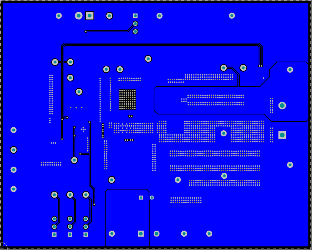 Figure 4-9 Bottom Layer