SLUUCK6A December 2021 – February 2022 TPSM8D6C24
- Trademarks
- 1 Description
- 2 Electrical Performance Specifications
- 3 Schematic
- 4 Test Setup
- 5 EVM Configuration Using the Fusion GUI
- 6 Test Procedure
- 7 Performance Data and Typical Characteristic Curves
- 8 EVM Assembly Drawing and PCB Layout
- 9 Bill of Materials
- 10Using the Fusion GUI
- 12Revision History
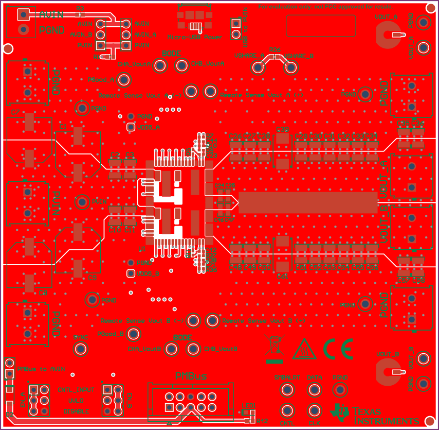
8 EVM Assembly Drawing and PCB Layout
Figure 8-1 through Figure 8-8 show the design of the TPSM8D6C24EVM-2V0 printed circuit board.
 Figure 8-1 TPSM8D6C24EVM-2V0 Top Side Component View (Top View)
 Figure 8-3 TPSM8D6C24EVM-2V0 Top Copper (Top
View)
 Figure 8-5 TPSM8D6C24EVM-2V0 Internal Layer 2
(Top View)
 Figure 8-7 TPSM8D6C24EVM-2V0 Internal Layer 4
(Top View)
 Figure 8-9 TPSM8D6C24EVM-2V0 Internal Layer 6
(Top View)
 Figure 8-2 TPSM8D6C24EVM-2V0 Bottom Side Component View (Bottom View)
 Figure 8-4 TPSM8D6C24EVM-2V0 Internal Layer 1
(Top View)
 Figure 8-6 TPSM8D6C24EVM-2V0 Internal Layer 3
(Top View)
 Figure 8-8 TPSM8D6C24EVM-2V0 Internal Layer 5
(Top View)
 Figure 8-10 TPSM8D6C24EVM-2V0 Internal Bottom
Layer (Top View)