SLUUCY8 December 2023 BQ77307
- 1
- Read This First
- 1 Introduction
- 2 Device Description
- 3 Device Configuration
- 4 Device Security
-
5 Protection
Subsystem
- 5.1 Protections Overview
- 5.2 Protection Evaluation and Detection
- 5.3 Protection FET Drivers
- 5.4 Cell Overvoltage Protection
- 5.5 Cell Undervoltage Protection
- 5.6 Short Circuit in Discharge Protection
- 5.7 Overcurrent in Charge Protection
- 5.8 Overcurrent in Discharge 1 and 2 Protections
- 5.9 Current Protection Latch
- 5.10 CHG Detector
- 5.11 Overtemperature in Charge Protection
- 5.12 Overtemperature in Discharge Protection
- 5.13 Internal Overtemperature Protection
- 5.14 Undertemperature in Charge Protection
- 5.15 Undertemperature in Discharge Protection
- 5.16 Cell Open Wire Detection
- 5.17 Voltage Reference Diagnostic Protection
- 5.18 VSS Diagnostic Protection
- 5.19 REGOUT Diagnostic Protection
- 5.20 LFO Oscillator Integrity Diagnostic Protection
- 5.21 Internal Factory Trim Diagnostic Protection
- 6 Device Status and Controls
- 7 Operational Modes
- 8 I2C Serial Communications
- 9 Commands and Subcommands
-
10Data Memory
- 10.1
Settings
- 10.1.1
Settings:Configuration
- 10.1.1.1 Settings:Configuration:Reserved
- 10.1.1.2 Settings:Configuration:Power Config
- 10.1.1.3 Settings:Configuration:REGOUT Config
- 10.1.1.4 Settings:Configuration:I2C Address
- 10.1.1.5 Settings:Configuration:I2C Config
- 10.1.1.6 Settings:Configuration:TS Mode
- 10.1.1.7 Settings:Configuration:Vcell Mode
- 10.1.1.8 Settings:Configuration:Default Alarm Mask
- 10.1.1.9 Settings:Configuration:FET Options
- 10.1.1.10 Settings:Configuration:Charge Detector Time
- 10.1.2
Settings:Protection
- 10.1.2.1 Settings:Protection:Enabled Protections A
- 10.1.2.2 Settings:Protection:Enabled Protections B
- 10.1.2.3 Settings:Protection:DSG FET Protections A
- 10.1.2.4 Settings:Protection:CHG FET Protections A
- 10.1.2.5 Settings:Protection:Both FET Protections B
- 10.1.2.6 Settings:Protection:Cell Open Wire Check Time
- 10.1.1
Settings:Configuration
- 10.2
Protections
- 10.2.1
Protections:Cell Voltage
- 10.2.1.1 Protections:Cell Voltage:Cell Undervoltage Protection Threshold
- 10.2.1.2 Protections:Cell Voltage:Cell Undervoltage Protection Delay
- 10.2.1.3 Protections:Cell Voltage:Cell Undervoltage Protection Recovery Hysteresis
- 10.2.1.4 Protections:Cell Voltage:Cell Overvoltage Protection Threshold
- 10.2.1.5 Protections:Cell Voltage:Cell Overvoltage Protection Delay
- 10.2.1.6 Protections:Cell Voltage:Cell Overvoltage Protection Recovery Hysteresis
- 10.2.2
Protections:Current
- 10.2.2.1 Protections:Current:Overcurrent in Charge Protection Threshold
- 10.2.2.2 Protections:Current:Overcurrent in Charge Protection Delay
- 10.2.2.3 Protections:Current:Overcurrent in Discharge 1 Protection Threshold
- 10.2.2.4 Protections:Current:Overcurrent in Discharge 1 Protection Delay
- 10.2.2.5 Protections:Current:Overcurrent in Discharge 2 Protection Threshold
- 10.2.2.6 Protections:Current:Overcurrent in Discharge 2 Protection Delay
- 10.2.2.7 Protections:Current:Short Circuit in Discharge Protection Threshold
- 10.2.2.8 Protections:Current:Short Circuit in Discharge Protection Delay
- 10.2.2.9 Protections:Current:Latch Limit
- 10.2.2.10 Protections:Current:Recovery Time
- 10.2.3
Protections:Temperature
- 10.2.3.1 Protections:Temperature:Overtemperature in Charge Protection Threshold
- 10.2.3.2 Protections:Temperature:Overtemperature in Charge Protection Delay
- 10.2.3.3 Protections:Temperature:Overtemperature in Charge Protection Recovery
- 10.2.3.4 Protections:Temperature:Undertemperature in Charge Protection Threshold
- 10.2.3.5 Protections:Temperature:Undertemperature in Charge Protection Delay
- 10.2.3.6 Protections:Temperature:Undertemperature in Charge Protection Recovery
- 10.2.3.7 Protections:Temperature:Overtemperature in Discharge Protection Threshold
- 10.2.3.8 Protections:Temperature:Overtemperature in Discharge Protection Delay
- 10.2.3.9 Protections:Temperature:Overtemperature in Discharge Protection Recovery
- 10.2.3.10 Protections:Temperature:Undertemperature in Discharge Protection Threshold
- 10.2.3.11 Protections:Temperature:Undertemperature in Discharge Protection Delay
- 10.2.3.12 Protections:Temperature:Undertemperature in Discharge Protection Recovery
- 10.2.3.13 Protections:Temperature:Internal Overtemperature Protection Threshold
- 10.2.3.14 Protections:Temperature:Internal Overtemperature Protection Delay
- 10.2.3.15 Protections:Temperature:Internal Overtemperature Protection Recovery
- 10.2.1
Protections:Cell Voltage
- 10.3 Power
- 10.4 Security
- 10.1
Settings
- 11Revision History
8.1 I2C Serial Communications Interface
The I2C serial communications interface in the BQ77307 device acts as a target device and supports rates up to 400 kHz with an optional CRC check. The BQ77307 initially powers up by default with CRC disabled, which is determined by the OTP settings factory programmed by TI. The host can change the CRC mode setting while in CONFIG_UPDATE mode, then the new setting takes effect upon exit of CONFIG_UPDATE mode.
The I2C device address (as an 8-bit value including target address and R/W bit) is set by default as 0x10 (write), 0x11 (read), which can be changed by the Settings:Configuration:I2C Address configuration setting.
The communications interface includes programmable timeout capability, with the internal I2C bus logic reset when an enabled timeout occurs:
- SCL Short Low Timeout - triggers if SCL stays low for approximately 25 ms. Enabled when Settings:Configuration:I2C Config[I2CCSLTO] is set.
- SCL Long Low Timeout - triggers if SCL stays low for a duration given by TLLO. TLLO is programmable using Settings:Configuration:I2C Config[I2CLLTOT2:0] as 0x0 = timeout is disabled, 0x1 = 0.5 sec, 0x2 = 1 sec, 0x3 = 1.5 sec, 0x4 = 2 sec, 0x5 = 2.5 sec, 0x6 = 3 sec, 0x7 = 3.5 sec. To use this timeout, Settings:Configuration:I2C Config[I2CLLTO] must be cleared.
An I2C write transaction is shown in I2C Write. Block writes are allowed by sending additional data bytes before the Stop. The I2C logic auto-increments the register address after each data byte. The shaded regions show when the device can clock stretch.

Figure 8-1 I2C Write
The CRC check is enabled by setting the Settings:Configuration:I2C Config[CRC] data memory bit. When enabled, the CRC is calculated as follows:
- The CRC is reset after each data byte and after each stop.
- In a single-byte write transaction, the CRC is calculated over the target address, register address, and data.
- In a block write transaction, the CRC for the first data byte is calculated over the target address, register address, and data. The CRC for subsequent data bytes is calculated over the data byte only.
The CRC polynomial is x8 + x2 + x + 1, and the initial value is 0.
When the target detects an invalid CRC, the I2C target NACKs the CRC, which causes the I2C target to go to an idle state.
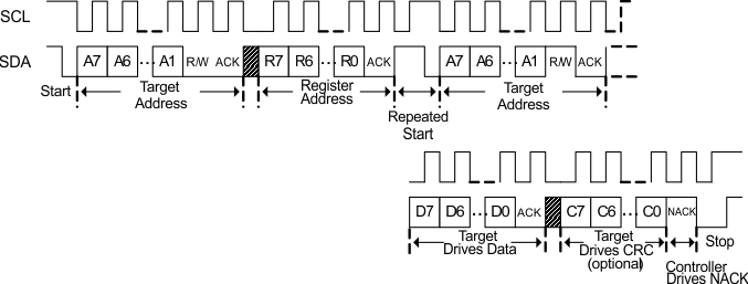
I2C Read with Repeated Start shows a read transaction using a Repeated Start. The shaded regions show when the device can clock stretch.

Figure 8-2 I2C Read with Repeated Start
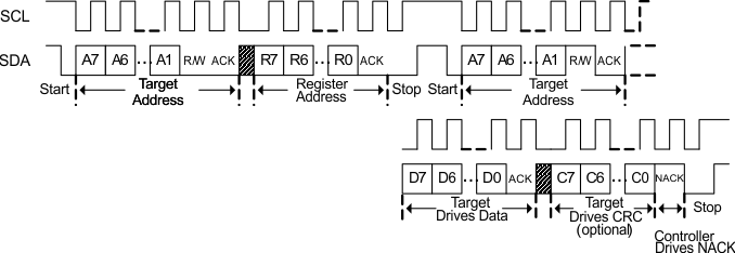
I2C Read without Repeated Start shows a read transaction where a Repeated Start is not used, for example if not available in hardware. For a block read, the controller ACKs each data byte except the last and continues to clock the interface. The I2C block auto-increments the register address after each data byte. The shaded regions show when the device can clock stretch.

Figure 8-3 I2C Read without Repeated Start
When enabled, the CRC for a read transaction is calculated as follows:
- The CRC is reset after each data byte and after each stop.
- In a single-byte read transaction using a repeated start, the CRC is calculated beginning at the first start, so includes the target address, the register address, then the target address with read bit set, then the data byte.
- In a single-byte read transaction using a stop after the initial register address, the CRC is reset after the stop, so only includes the target address with read bit set and the data byte.
- In a block read transaction using repeated starts, the CRC for the first data byte is calculated beginning at the first start and includes the target address, the register address, then the target address with read bit set, then the data byte. The CRC for subsequent data bytes is calculated over the data byte only.
- In a block read transaction using a stop after the initial register address, the CRC is reset after the stop, so only includes the target address with read bit set and the first data byte. The CRC for subsequent data bytes is calculated over the data byte only.
The CRC polynomial is x8 + x2 + x + 1, and the initial value is 0.
When the controller detects an invalid CRC, the I2C controller NACKs the CRC, which causes the I2C target to go to an idle state.