SLUUD38 June   2024 TPSM82866A , TPSM82866C


  1.   1
  2.   Description
  3.   Features
  4.   4
  5. 1Evaluation Module Overview
    1. 1.1 Introduction
    2. 1.2 Kit Contents
    3. 1.3 Specification
    4. 1.4 Device Information
  6. 2Hardware
    1. 2.1 Safety Instructions
    2. 2.2 Header Information
    3. 2.3 Jumper Information
    4. 2.4 Interfaces
    5. 2.5 Test Points
  7. 3Software
  8. 4Implementation Results
    1. 4.1 Evaluation Setup
      1. 4.1.1 VSET/VID Resistor (TPSM82866CA3PEVM only)
      2. 4.1.2 VSET/MODE Resistor (TPSM82866AA0PEVM only)
      3. 4.1.3 Input and Output Capacitors
      4. 4.1.4 Feedforward Capacitor
      5. 4.1.5 Loop Response Measurement
    2. 4.2 Performance Data and Results
  9. 5Hardware Design Files
    1. 5.1 Schematics
    2. 5.2 PCB Layouts
    3. 5.3 Bill of Materials (BOM)
  10. 6Additional Information
    1. 6.1 Trademarks

Loop Response Measurement

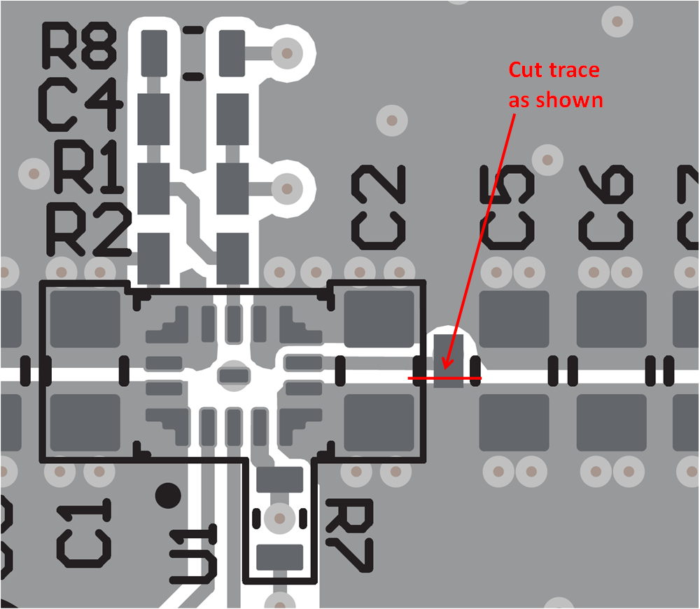
The loop response can be measured with simple changes to the circuitry. First, install a 10Ω resistor across the pads of R6 on the back of the PCB. The pads are spaced to allow installation of an 0603-sized resistor. Next, cut the short section of trace on the top layer between C2 and C5 to separate the via on VOUT from the plane. Figure 5-1 shows this cut. With these changes, an AC signal (10mV, peak-to-peak amplitude recommended) can be injected into the control loop across the added 10Ω resistor. Figure 5-4 shows the results of this test.
TPSM82866AA0PEVM, TPSM82866CA3PEVM Loop Response Measurement ModificationFigure 4-1 Loop Response Measurement Modification