SLVAFB4 July 2022 TPS62902-Q1 , TPS62903 , TPS62903-Q1
1.1 Concept
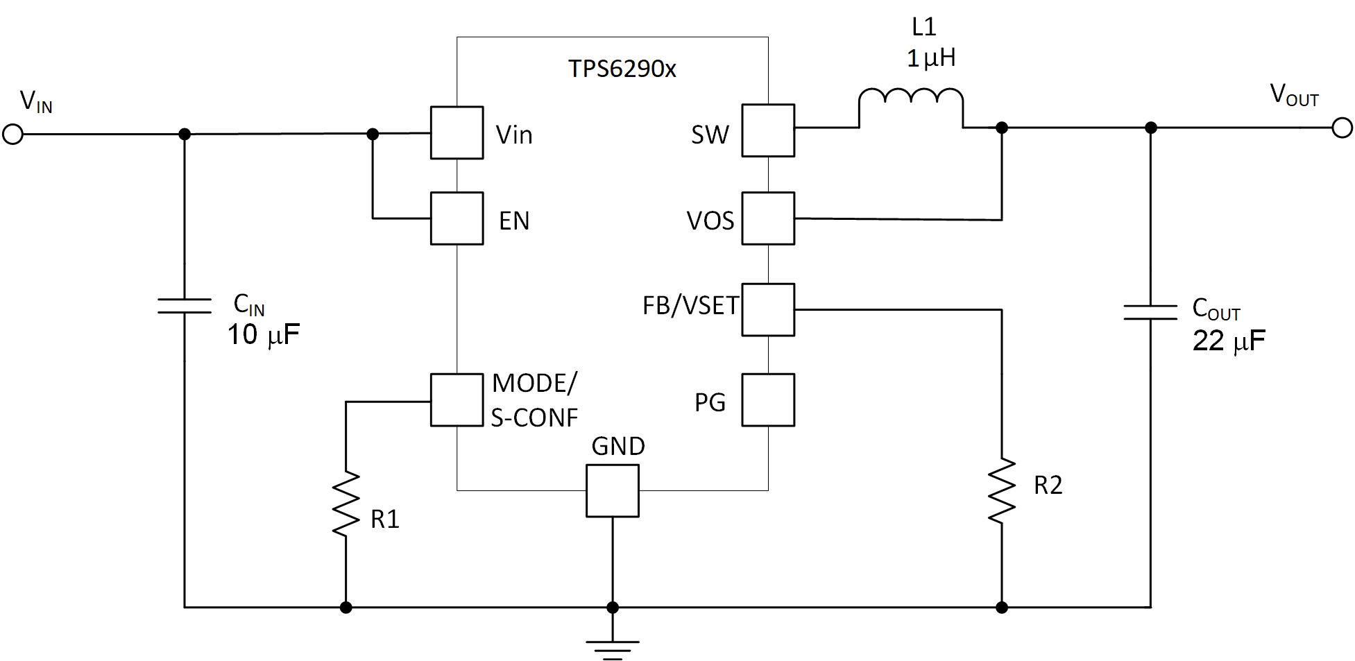
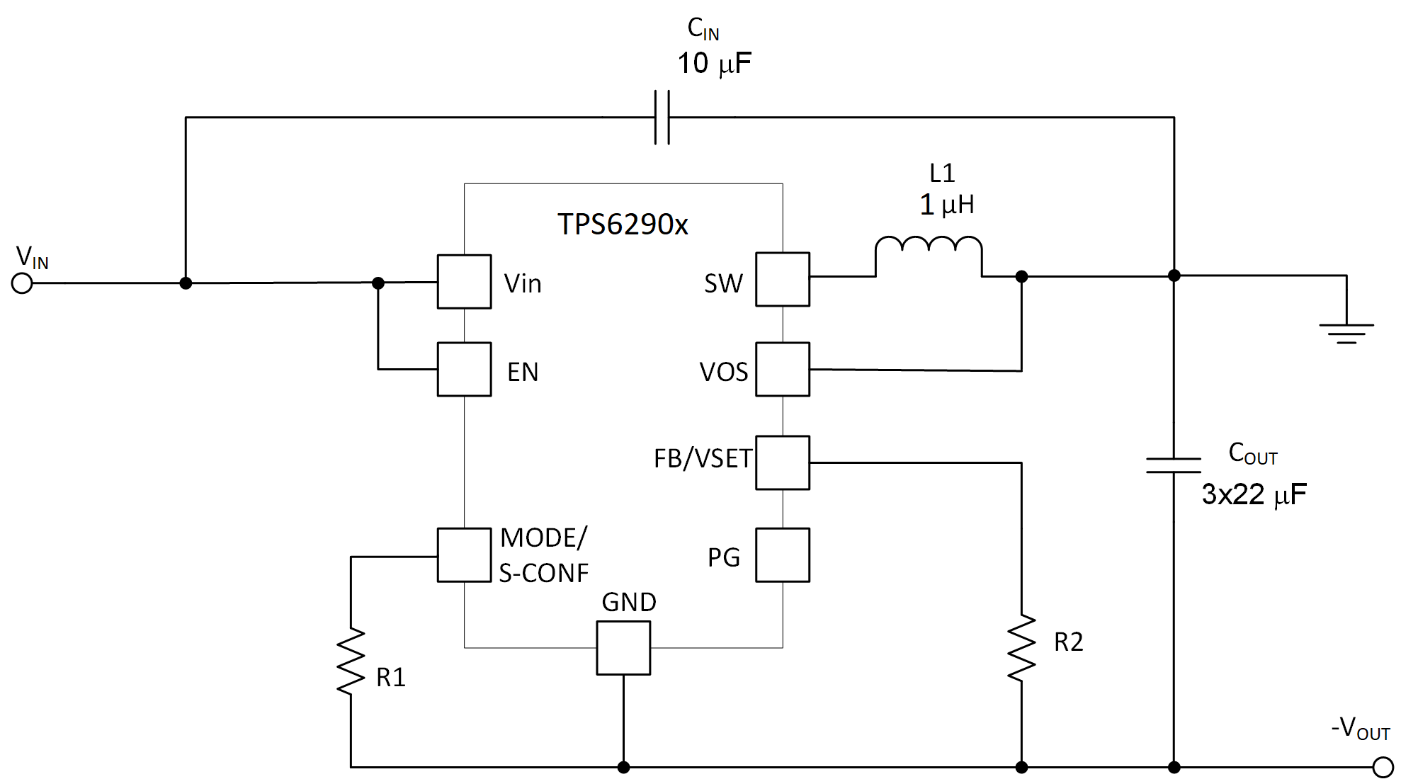
The inverting buck – boost topology is very similar to the buck topology. In the buck configuration shown in Figure 1-1, the positive connection (VOUT) is connected to the inductor and the return is connected to the integrated circuit (IC) ground. However, in the inverting buck – boost configuration shown in Figure 1-2, the IC ground is used as the negative output voltage (labeled as -VOUT). What used to be the positive output in buck configuration is used as the ground (GND). This inverting buck – boost topology allows the output voltage to be inverted and is always lower than the ground.
 Figure 1-1 TPS62903 Buck Topology
 Figure 1-2 TPS62903 Inverting Buck – Boost
Topology
Figure 1-2 TPS62903 Inverting Buck – Boost
TopologyThe circuit operation is different in the inverting buck - boost topology than in the buck topology. Figure 1-3 (a) illustrates that the output voltage terminals are reversed, though the components are wired the same as a buck converter. During the on time of the control MOSFET, shown in Figure 1-3 (b), the inductor is charged with current while the output capacitor supplies the load current. The inductor does not provide current to the load during that time. During the off time of the control MOSFET and the on time of the synchronous MOSFET, shown in Figure 1-3 (c), the inductor provides current to the load and the output capacitor. These changes affect many parameters described in the upcoming sections.
 Figure 1-3 Inverting Buck – Boost Configuration