SLVAFB4 July 2022 TPS62902-Q1 , TPS62903 , TPS62903-Q1
2.1 Enable Pin
The TPS62903 is enabled once the voltage at the EN pin trips its threshold and the input voltage is above the UVLO threshold. The device stops operation once the voltage on the EN pin falls below its threshold or the input voltage falls below UVLO threshold.
Because -VOUT is the IC ground in this configuration, the EN pin must be referenced to -VOUT instead of ground. In the buck configuration, 1 V is considered to turn on and less than 0.9 V is considered to turn off. In the inverting buck-boost configuration, however, the -VOUT voltage is the reference; therefore, the high threshold is 1 V + VOUT and the low threshold is 0.9 V + VOUT. Where VOUT is a negative value. For example, if VOUT = –3.3 V, the VEN is considered at a high level for voltages above –2.3 V and at a low level for voltages below –2.4 V.
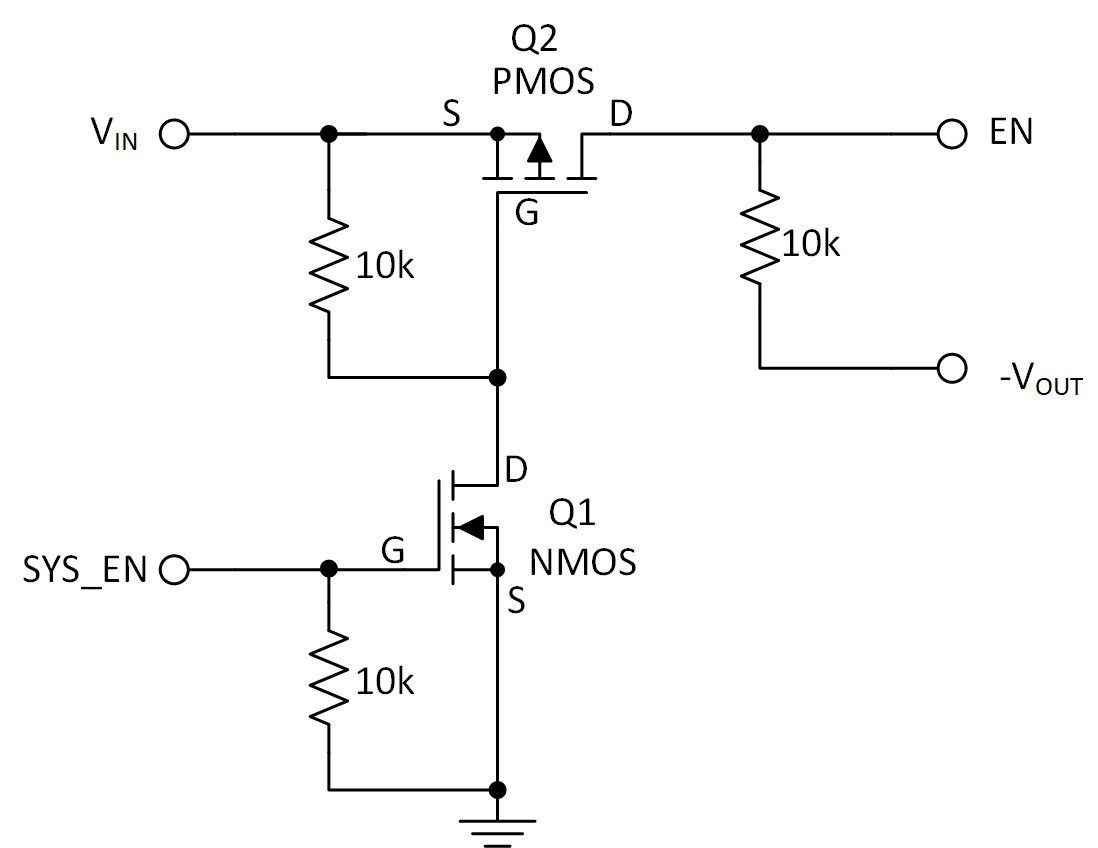
This behavior can cause difficulties enabling or disabling the device, since in some applications, the IC providing the EN signal might not be able to produce negative voltages. The level shifter circuit shown in Figure 2-1 alleviates any difficulties associated with the offset EN threshold voltages by eliminating the need for negative EN signals.

The positive signal (SYS_EN) that originally drove EN is instead tied to the gate of Q1. When Q1 is off , Q2 sees 0 V across its VGS, and also remains off. In this state, the EN pin sees –3.3 V for -VOUT= - 3.3 V which is below the low level threshold and it disables the device.
When SYS_EN provides enough positive voltage to turn Q1 on (VGS threshold as specified in the MOSFET data sheet), the gate of Q2 sees ground through Q1. This drives the VGS of Q2 negative and turns Q2 on. Now, VIN ties to EN through Q2 and the pin is above the high level threshold, turning the device on. Be careful to ensure that the VGD and VGS of Q2 remain within the MOSFET ratings during both the enabled and disabled states. Failing to adhere to this constraint might result in MOSFET damage. A small size complementary N and P Channel 60V (D-S) MOSFET Si1029X from Vishay can be used in the design.
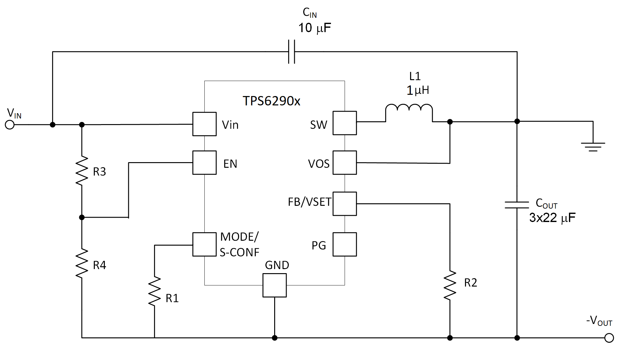
If the system enabling and disabling of the TPS62903 is not desired, the EN pin can be directly connected to VIN or a voltage divider connected to VIN. We strongly recommend to add a voltage divider placeholder (R3/R4) between VIN and EN pin which is shown in Figure 2-2. Recommend R3:R4≥2:1 ratio to ensure VIN >2.95 V UVLO before EN> 1V which the internal circuit of device is ready before EN is fully enabled. UVLO and EN falling thresholds become relative to -VOUT instead of GND . For example, UVLO falling=2.75 V +VOUT and EN falling= 0.9 V + VOUT. Where VOUT is a negative value. Customer can scale the voltage divider R3/R4 ratio based on the real application. This is a reliable solution to eliminate any start up and shut down related issues.
 Figure 2-2 EN Pin with Voltage
Divider