SLVAFP0 December   2023 LMR51610


  1.   1
  2.   Abstract
  3.   Trademarks
  4. 1Introduction
  5. 2Specifications
    1. 2.1 Input Voltage Range
    2. 2.2 Output Current Range
  6. 3External Component Selection
    1. 3.1 Duty Cycle Calculation
    2. 3.2 Output Voltage Calculation
    3. 3.3 Inductor Selection
    4. 3.4 Input and Output Capacitor
    5. 3.5 Enable Level Shift
    6. 3.6 Output Clamp Diode
  7. 4Evaluation Results
    1. 4.1 Typical Performance
    2. 4.2 Loop Response Bench Verification
  8. 5Conclusion
  9. 6References
  10. 7LMR50410 Design Example
    1. 7.1 LMR50410 Output Current Range
    2. 7.2 LMR50410 Efficiency

Input Voltage Range

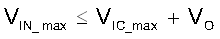
The LMR51610 IC can tolerate 65v Vin max voltage, however in the IBB circuit the input voltage ability is not only limited by the device, but also related with the -Vout, use Equation 1 to calculate the input voltage.

Equation 1. GUID-F1F9ECE7-2A66-4D14-B87A-13A9ED27DAF6-low.gif

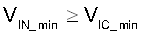
The minimum operating input voltage of the inverting power supply is the minimum device operating voltage, see Equation 2. For LMR51610 the minimum input voltage is 4 V, so the inverting power supply input voltage must be higher than 4 V.

Equation 2. GUID-F98520A6-6A4F-4DE2-A636-8273C672BF3B-low.gif