SLVAFP0 December 2023 LMR51610
4.1 Typical Performance
Figure 7-17 to Figure 4-13 show the experimental test results of the Figure 3-3 design. Unless otherwise specified, the following conditions apply: VIN = 24 V, VO = -12 V, IO = 0.4 A, TA = 25 °C.
 Figure 4-1 Efficiency vs Load Current Vout=-5 V
 Figure 4-3 Line Regulation Vout=-5 V
 Figure 4-5 Load Regulation Vout=-5 V
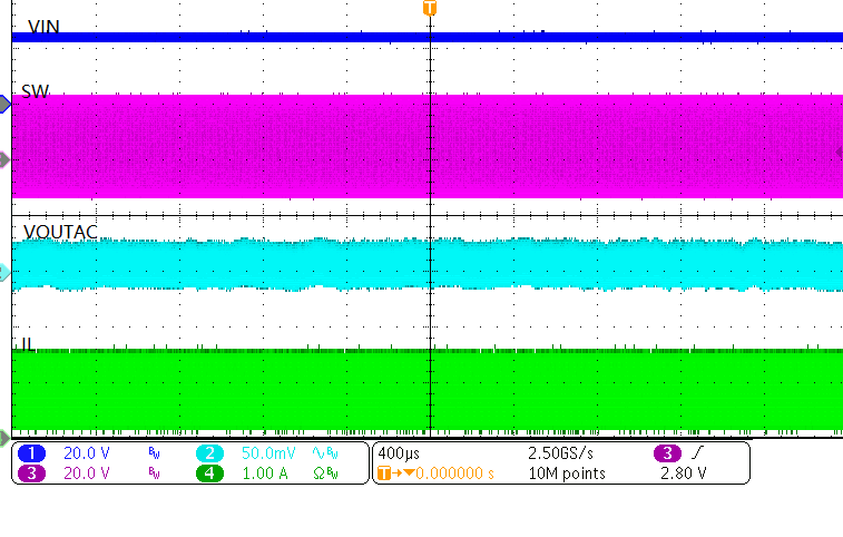 Figure 4-7 Output Voltage Ripple at no Load
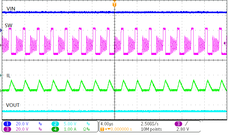 Figure 4-9 Steady States at Light Load 100 mA
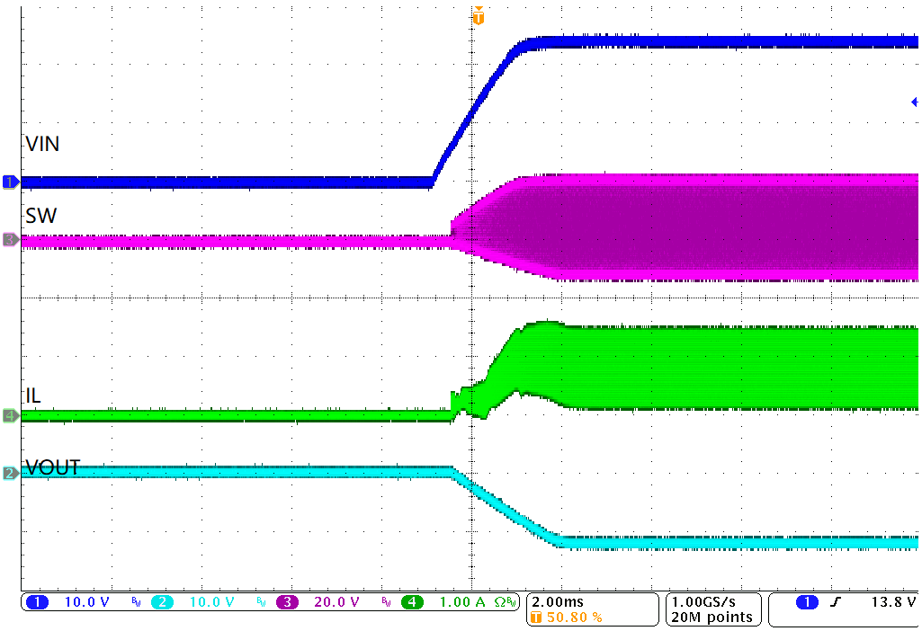 Figure 4-11 Start Up by Vin 500mA Load
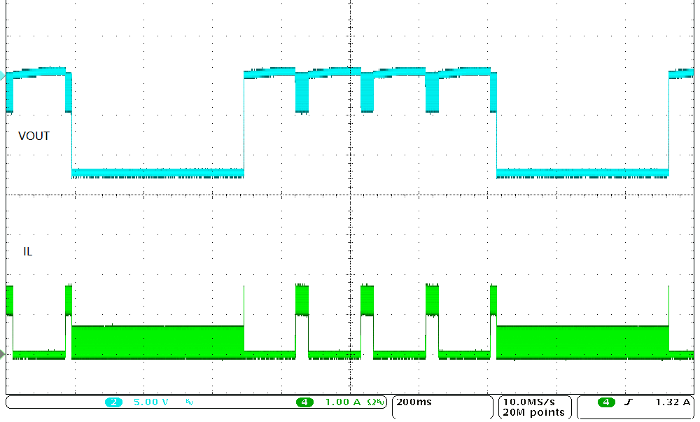 Figure 4-13 Over Current Protection
 Figure 4-2 Efficiency vs Load Current Vout=-12 V
 Figure 4-4 Line Regulation Vout=-12 V
 Figure 4-6 Load Regulation Vout=-12 V
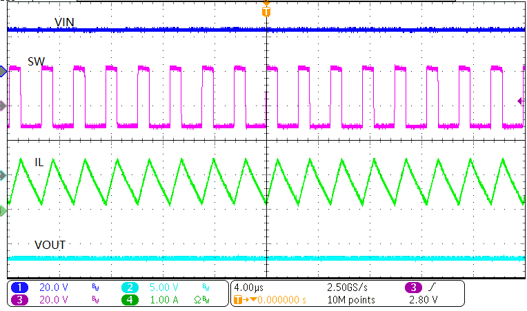 Figure 4-8 Steady States at Full Load 500mA
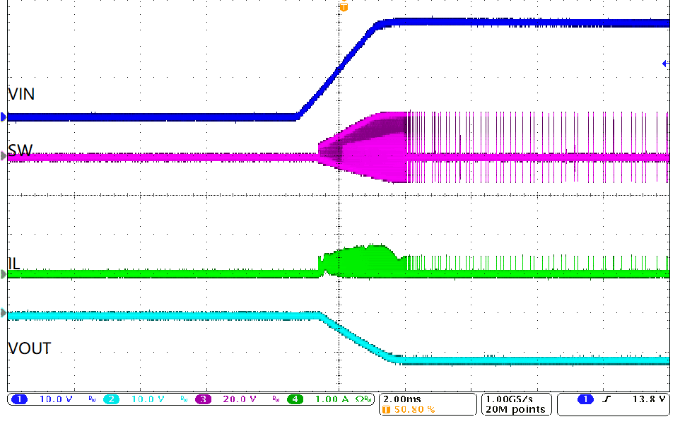 Figure 4-10 Start Up by Vin no Load
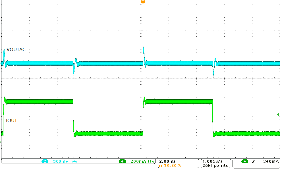 Figure 4-12 Load Transient 100mA to 500mA