SLVAFV5 July 2024 TLV62095
Overview
This document contains the Pin failure mode analysis (pin FMA) information for the TLV62095.
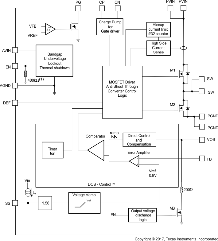
Figure 1 shows the device functional block diagram.
 Figure 1 Functional Block Diagram
Pin Failure Mode Analysis (Pin FMA)
This section provides a failure mode analysis (FMA) for the pins of the TLV62095. The failure modes covered in this document include the typical pin-by-pin failure scenarios:
- Pin short-circuited to ground (see Table 2)
- Pin open-circuited (see Table 3)
- Pin short-circuited to an adjacent pin (see Table 4)
- Pin short-circuited to VIN (see Table 5)
Table 2 through Table 5 also indicate how these pin conditions can affect the device as per the failure effects classification in Table 1.
| Class | Failure Effects |
|---|---|
| A | Potential device damage that affects functionality. |
| B | No device damage, but loss of functionality. |
| C | No device damage, but performance degradation. |
| D | No device damage, no impact to functionality or performance. |
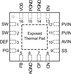
Table 2 is showing the TLV62095 pin diagram. For a detailed description of the device pins, see the Pin Configuration and Functions section in the TLV62095 4-A High Efficiency Step Down Converter with DCS-Control Data Sheet.
 Figure 2 Pin Diagram
The exposed thermal pad is connected to AGND.
Following are the assumptions of use and the device configuration assumed for the pin FMA in this section:
- The device is operating in the typical application, see the Applications section on the first page in the TLV62095 4-A High Efficiency Step Down Converter with DCS-Control Data Sheet.
| Pin Name | Pin No. | Description of Potential Failure Effect(s) | Failure Effect Class |
|---|---|---|---|
| SW | 1, 2 | Potential internal device damage | A |
| DEF | 3 | Incorrect device functionality due to different switching frequency | B |
| PG | 4 | No impact on device | D |
| FB | 5 | Incorrect device functionality due to missing feedback path | B |
| AGND | 6 | Intended connection | D |
| CP | 7 | Potential impact on device reliability; potential internal device damage | A |
| CN | 8 | Potential impact on device reliability; potential internal device damage | A |
| SS | 9 | Incorrect device functionality; Device does not start up | B |
| AVIN | 10 | Potential damage | A |
| PVIN | 11, 12 | Potential damage | A |
| EN | 13 | Device disabled | D |
| PGND | 14, 15 | Intended connection | D |
| VOS | 16 | Reduced transient performance; no output discharge available; reduced current limit | B |
| Pin Name | Pin No. | Description of Potential Failure Effect(s) | Failure Effect Class |
|---|---|---|---|
| SW | 1 | Increased current through pin (2); potential impact on device reliability; potential damage | A |
| SW | 2 | Increased current through pin (1); potential impact on device reliability; potential damage | A |
| DEF | 3 | Incorrect device functionality due to different switching frequency | B |
| PG | 4 | Intended operation if PG not used | D |
| FB | 5 | Incorrect device functionality due to missing feedback path | B |
| AGND | 6 | Incorrect device functionality due to missing AGND connection | B |
| CP | 7 | Incorrect device functionality | B |
| CN | 8 | Incorrect device functionality | B |
| SS | 9 | Intended operation; sets minimum soft start time (typ 50us) | D |
| AVIN | 10 | Device not functional | B |
| PVIN | 11 | Increased current through pin (12); potential impact on device reliability; potential internal device damage | A |
| PVIN | 12 | Increased current through pin (11); potential impact on device reliability; potential internal device damage | A |
| EN | 13 | Intended operation; internal pull-down keeps this pin low; device disabled. | D |
| PGND | 14 | Increased current through pin (15); potential impact on device reliability; potential internal device damage | A |
| PGND | 15 | Increased current through pin (14); potential impact on device reliability; potential internal device damage | A |
| VOS | 16 | Reduced transient performance; no output discharge available; potentially reduced current limit | B |
| Pin Name | Pin No. | Shorted to | Pin No. | Description of Potential Failure Effect(s) | Failure Effect Class |
|---|---|---|---|---|---|
| SW | 1 | SW | 2 | Intended connection | D |
| SW | 2 | DEF | 3 | Potential internal device damage through potential violation of abs max voltage rating of pin (3) | A |
| DEF | 3 | PG | 4 | Potential internal device damage through potential violation of abs max voltage rating of pin (3) | A |
| PG | 4 | FB | 5 | Incorrect device functionality due to disturbed feedback path; potential internal device damage through potential violation of abs max voltage rating of pin (5) | A |
| FB | 5 | AGND | 6 |
Incorrect device functionality due to missing feedback path. |
B |
| AGND | 6 | CP | 7 | Potential impact on device reliability; potential internal device damage | A |
| CP | 7 | CN | 8 | Incorrect device functionality; potential impact on device reliability | A |
| CN | 8 | SS | 9 | Incorrect device functionality | B |
| SS | 9 | AVIN | 10 | Sets minimum soft start time (typ 50us) | B |
| AVIN | 10 | PVIN | 11 | Potentially incorrect device functionality due to increased disturbance of AVIN supply by ringing on PVIN pin | B |
| PVIN | 11 | PVIN | 12 | Intended connection | D |
| PVIN | 12 | EN | 13 | Intended connection; device is enabled with VIN>UVLO | D |
| EN | 13 | PGND | 14 | Intended operation; device disabled. | D |
| PGND | 14 | PGND | 15 | Intended connection | D |
| PGND | 15 | VOS | 16 | Output short to ground, device not functional | B |
| VOS | 16 | SW | 1 | Incorrect device functionality | B |
| Pin Name | Pin No. | Description of Potential Failure Effect(s) | Failure Effect Class |
|---|---|---|---|
| SW | 1, 2 | Potential internal device damage | A |
| DEF | 3 | Intended operation; nominal switching frequency set to 1.4MHz | D |
| PG | 4 | Potential internal device damage | A |
| FB | 5 | Incorrect device functionality due to missing feedback path. | B |
| AGND | 6 | Internal damage | A |
| CP | 7 | Potential impact on device reliability; potential internal device damage | A |
| CN | 8 | Potential impact on device reliability; potential internal device damage | A |
| SS | 9 | Sets minimum soft start time (typ 50us) | D |
| AVIN | 10 | Intended connection | D |
| PVIN | 11, 12 | Intended connection | D |
| EN | 13 | Intended operation; device always enabled | D |
| PGND | 14, 15 | Potential damage | A |
| VOS | 16 | Potential internal device damage | A |