SLVS417F March   2002  – June 2015

PRODUCTION DATA.  

  1. Features
  2. Applications
  3. Description
  4. Revision History
  5. Pin Configuration and Functions
  6. Specifications
    1. 6.1 Absolute Maximum Ratings
    2. 6.2 ESD Ratings
    3. 6.3 Recommended Operating Conditions
    4. 6.4 Thermal Information
    5. 6.5 Electrical Characteristics
    6. 6.6 Typical Characteristics
  7. Detailed Description
    1. 7.1 Overview
    2. 7.2 Functional Block Diagram
    3. 7.3 Feature Description
      1. 7.3.1 Undervoltage Lockout
      2. 7.3.2 Dynamic Voltage Positioning
      3. 7.3.3 Soft Start
      4. 7.3.4 Low Dropout Operation 100% Duty Cycle
      5. 7.3.5 Enable
    4. 7.4 Device Functional Modes
      1. 7.4.1 Power Save Mode Operation
  8. Application and Implementation
    1. 8.1 Application Information
    2. 8.2 Typical Application
      1. 8.2.1 Design Requirements
      2. 8.2.2 Detailed Design Procedure
        1. 8.2.2.1 Adjustable Output Voltage Version
        2. 8.2.2.2 Inductor Selection
        3. 8.2.2.3 Input Capacitor Selection
        4. 8.2.2.4 Output Capacitor Selection
      3. 8.2.3 Application Curves
    3. 8.3 System Examples
      1. 8.3.1 Various Output Voltages
      2. 8.3.2 Adjustable Output Voltage Version Set to 1.5 V
  9. Power Supply Recommendations
  10. 10Layout
    1. 10.1 Layout Guidelines
    2. 10.2 Layout Example
  11. 11Device and Documentation Support
    1. 11.1 Device Support
      1. 11.1.1 Third-Party Products Disclaimer
    2. 11.2 Related Links
    3. 11.3 Community Resources
    4. 11.4 Trademarks
    5. 11.5 Electrostatic Discharge Caution
    6. 11.6 Glossary
  12. 12Mechanical, Packaging, and Orderable Information

5 Pin Configuration and Functions

DBV Package
5-Pin SOT-23
Top View
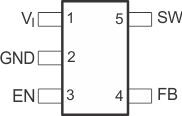
TPS62200 TPS62201 TPS62202 TPS62203 TPS62204 TPS62205 TPS62207 TPS62208 po_dbv_lvs417.gif

Pin Functions

PIN I/O DESCRIPTION
NAME NO.
EN 3 I This is the enable pin of the device. Pulling this pin to ground forces the device into shutdown mode. Pulling this pin to Vin enables the device. This pin must not be left floating and must be terminated.
FB 4 I This is the feedback pin of the device. Connect this pin directly to the output if the fixed output voltage version is used. For the adjustable version an external resistor divider is connected to this pin. The internal voltage divider is disabled for the adjustable version.
GND 2 Ground
SW 5 I/O Connect the inductor to this pin. This pin is the switch pin and is connected to the internal MOSFET switches.
VI 1 I Supply voltage pin