TPS61045 Digitally Adjustable Boost Converter
1 Features
- Input Voltage Range from 1.8 to 6 V
- Output Voltage of up to 28 V Possible
- Up to 85% Efficiency
- Digitally Adjustable Output Voltage Control
- Disconnects Output From Input During Shutdown
- Switching Frequency up to 1 MHz
- No Load Quiescent Current 40 μA Typical
- Thermal Shutdown Mode
- Shutdown Current 0.1 μA Typical
- Available in Small 3-mm × 3-mm VSON Package
2 Applications
- LCD Bias Supply for Small to Medium LCD Displays
- OLED Display Power Supply
- PDA, Pocket PC, Smart Phones
- Handheld Devices
- Cellular Phones
3 Description
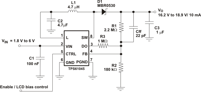
The TPS61045 device is a high-frequency boost converter with digitally-programmable output voltage and true shutdown. During shutdown, the output is disconnected from the input by opening the internal input switch. This allows a controlled power-up and power-down sequencing of the display. The output voltage can be increased or decreased in digital steps by applying a logic signal to the CTRL pin. The output voltage range, as well as the output voltage step size, can be programmed with the feedback divider network. With a high switching frequency of up to 1 MHz, the TPS61045 device allows the use of small external components, and together, with the small 8-pin VSON package, a minimum system solution size is achieved.
Device Information(1)
| PART NUMBER | PACKAGE | BODY SIZE (NOM) |
|---|---|---|
| TPS61045 | VSON (8) | 3.00 mm × 3.00 mm |
- For all available packages, see the orderable addendum at the end of the data sheet.
Simplified Schematic
4 Revision History
Changes from B Revision (March 2009) to C Revision
- Added ESD Ratings table, Feature Description section, Device Functional Modes, Application and Implementation section, Power Supply Recommendations section, Layout section, Device and Documentation Support section, and Mechanical, Packaging, and Orderable Information section Go
- Updated Equation 10Go
- Updated Equation 11Go
5 Pin Configuration and Functions

Pin Functions
| PIN | I/O | DESCRIPTION | |
|---|---|---|---|
| NAME | NO. | ||
| CTRL | 5 | I | Combined enable and digital output voltage programming pin. Pulling CTRL constantly high enables the device. When CTRL is pulled to GND, the device is disabled and the input is disconnected from the output by opening the integrated switch Q1. Pulsing CTRL low increases or decreases the output voltage. Refer to Application and Implementation for further information. |
| DO | 3 | O | Internal DAC output. DO programs the output voltage through the CTRL pin. Refer to Application and Implementation for further information. |
| FB | 4 | I | Feedback. FB must be connected to the output voltage-feedback divider. |
| GND | 6 | — | Analog ground. GND must be directly connected to the PGND pin. Refer to Application and Implementation for further information. |
| L | 1 | O | Drain of the internal input switch (Q1). Connect L to the inductor. |
| PGND | 7 | — | Power ground |
| SW | 8 | I | Drain of the integrated main switch Q2. SW is connected to the inductor and anode of the Schottky rectifier diode. |
| VIN | 2 | I | Input supply pin |
6 Specifications
6.1 Absolute Maximum Ratings
over operating free-air temperature (unless otherwise noted)(1)| MIN | MAX | UNIT | ||
|---|---|---|---|---|
| Supply voltage | VVIN(2) | –0.3 | 7 | V |
| Voltage | VCTRL, V(FB), VL, VDO(2) | –0.3 | VIN + 0.3 | V |
| Voltage | VSW(2) | 30 | V | |
| Continuous power dissipation | See Dissipation Rating | |||
| TJ | Operating junction temperature | –40 | 150 | °C |
| Tstg | Storage temperature | –65 | 150 | °C |
6.2 ESD Ratings
| VALUE | UNIT | |||
|---|---|---|---|---|
| V(ESD) | Electrostatic discharge | Human body model (HBM), per ANSI/ESDA/JEDEC JS-001, all pins(1) | ±1500 | V |
| Charged device model (CDM), per JEDEC specification JESD22-C101, all pins(2) | ±500 | |||
6.3 Recommended Operating Conditions
| MIN | TYP | MAX | UNIT | ||
|---|---|---|---|---|---|
| VVIN | Input voltage range | 1.8 | 6 | V | |
| VSW | Switch voltage | 30 | V | ||
| L | Inductor (1) | 4.7 | μH | ||
| ƒ | Switching frequency(1) | 1 | MHz | ||
| CI(C2) | Input capacitor (C2) (1) | 4.7 | μF | ||
| CO(C3) | Output capacitor (C3) (1) | 1 | μF | ||
| TA | Operating ambient temperature | –40 | 85 | °C | |
| TJ | Operating junction temperature | –40 | 125 | °C | |
6.4 Thermal Information
over operating free-air temperature range (unless otherwise noted)| THERMAL METRIC(1) | TPS61045 | UNIT | ||
|---|---|---|---|---|
| VSON (8 PINS) | ||||
| RΘJA(2) | Junction-to-ambient thermal resistance | 270 | °C/W | |
6.5 Dissipation Rating
| PACKAGE | TA ≤ 25°C POWER RATING |
DERATING FACTOR ABOVE TA = 25°C | TA = 70°C POWER RATING |
TA = 85°C POWER RATING |
|---|---|---|---|---|
| 8-pin VSON (DRB) (1) | 370 mW | 3.7 mW/°C | 204 mW | 148 mW |
6.6 Electrical Characteristics
VIN = 2.4 V, CTRL = VIN, VO = 18 V, IO = 10 mA, TA = –40°C to 85°C, typical values are at TA = 25° C (unless otherwise noted)| PARAMETER | TEST CONDITIONS | MIN | TYP | MAX | UNIT | |
|---|---|---|---|---|---|---|
| SUPPLY CURRENT | ||||||
| VIN | Input voltage range | 1.8 | 6 | V | ||
| IQ | Operating quiescent current | IO = 0 mA, not switching | 40 | 65 | μA | |
| IO(SD) | Shutdown current | CTRL = GND | 0.1 | 1 | μA | |
| UVLO | Undervoltage lockout (UVLO) threshold | VIN falling | 1.5 | 1.7 | V | |
| CTRL AND DAC OUTPUT | ||||||
| VIH | CTRL high-level input voltage | 1.3 | V | |||
| VIL | CTRL low-level input voltage | 0.3 | V | |||
| Ilkg | CTRL input leakage current | CTRL = GND or VIN | 0.1 | μA | ||
| VO(DO) | DAC output voltage range | 0 | 1.233 | V | ||
| DAC resolution | 6 bit | 19.6 | mV | |||
| VO(DO) | DAC center output voltage | CTRL = high | 607 | mV | ||
| IO(SINK) | Maximum DAC sink current | 30 | μA | |||
| tUP | Increase output voltage one step | CTRL = High to low to high | 1 | 60 | μs | |
| tDWN | Decrease the output voltage one step | CTRL = High to low to high | 140 | 240 | μs | |
| td1 | Delay time between up and down steps | CTRL = Low to high to low | 1 | μs | ||
| tOFF | Shutdown | CTRL = High to low to high | 560 | μs | ||
| INPUT SWITCH (Q1), MAIN SWITCH (Q2), AND CURRENT LIMIT | ||||||
| VSW(Q2) | Main switch maximum voltage (Q2) | 30 | V | |||
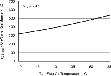
| rDS(on) | Main switch MOSFET on-resistance | VIN = 2.4 V; IS = 200 mA | 400 | 800 | mΩ | |
| Ilkg | Main switch MOSFET leakage current | VS = 28 V | 0.1 | 10 | μA | |
| ILIM | Main switch MOSFET current limit | 300 | 375 | 450 | mA | |
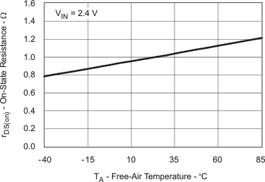
| rDS(on) | Input switch MOSFET on-resistance | VIN = 2.4 V; IS = 200 mA | 1 | 2 | Ω | |
| Ilkg | Input switch MOSFET leakage current | VL = GND, VIN = 6 V | 0.1 | 10 | μA | |
| OUTPUT | ||||||
| VO | Output voltage range | VIN | 28 | V | ||
| Vref | Internal voltage reference | 1.233 | V | |||
| IFB | Feedback input bias current | V(FB) = 1.3 V | 30 | 100 | nA | |
| VFB | Feedback trip point voltage | 1.8 V ≤ VIN ≤ 6 V; VO = 18 V, ILOAD = 10 mA | 1.208 | 1.233 | 1.258 | V |
| Feedback trip point voltage | 1.8 V ≤ VIN≤ 3.6 V; VO = 18 V, ILOAD = 10 mA , TA = 0°C to 85°C |
1.214 | 1.233 | 1.251 | V | |
6.7 Typical Characteristics
Table 1. Table of Graphs
| Graph Title | Figure | |
|---|---|---|
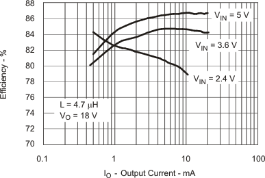
| η | Efficiency vs Load Current | Figure 1 |
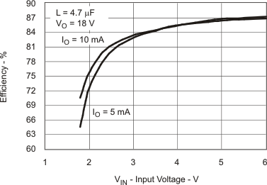
| Efficiency vs Input Voltage | Figure 2 | |
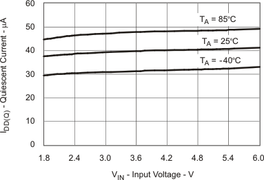
| IDD(Q) | Quiescent Current vs Input Voltage | Figure 3 |
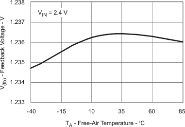
| VFB | Feedback Voltage vs Temperature | Figure 4 |
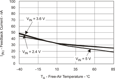
| IFB | Feedback Current vs Temperature | Figure 5 |
| rDS(on) | rDS(on) Main Switch Q2 vs Temperature | Figure 6 |
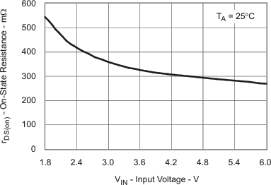
| rDS(on) Main Switch Q2 vs Input Voltage | Figure 7 | |
| rDS(on) Input Switch Q1 vs Temperature | Figure 8 | |
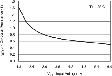
| rDS(on) Input Switch Q1 vs Input Voltage | Figure 9 | |
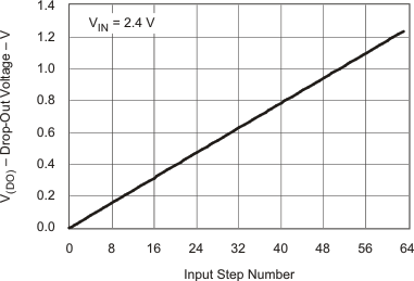
| VDO | VDO Voltage vs CTRL Input Step | Figure 10 |
| Line Transient Response | Figure 13 | |
| Load Transient Response | Figure 14 | |
| PFM Operation | Figure 15 | |
| Softstart | Figure 16 | |
7 Detailed Description
7.1 Overview
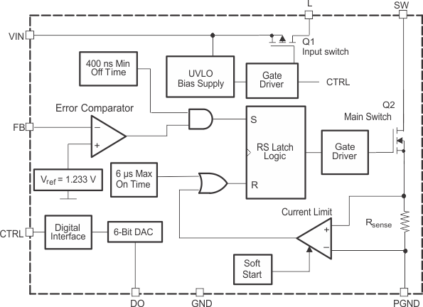
The TPS61045 device operates with an input voltage range of 1.8 to 6 V and generates output voltages up to 28 V. The device operates in a pulse frequency modulation (PFM) scheme with constant peak current control. This control scheme maintains high efficiency over the entire load current range, and with a switching frequency of up to 1 MHz, the device enables the use of small external components.
The converter monitors the output voltage. When the feedback voltage falls below the reference voltage of
1.233 V (typical), the main switch turns on and the current ramps up. The main switch turns off when the inductor current reaches the internally set peak current of 375 mA (typical). See Peak Current Control for more information. The second criteria that turns off the main switch is the maximum on-time of 6 μs (typical). This limits the maximum on-time of the converter in extreme conditions. As the switch is turned off, the external Schottky diode is forward biased delivering the current to the output. The main switch remains off until the minimum off time of 400 ns (typical) has passed and the feedback voltage is below the reference voltage again. Using this PFM peak current control scheme, the converter operates in discontinuous conduction mode (DCM) where the switching frequency depends on the input voltage, output voltage, and output current. This gives a high efficiency over the entire load current range. This regulation scheme is inherently stable, which allows a wider range for the selection of the inductor and output capacitor.
7.2 Functional Block Diagram
7.3 Feature Description
7.3.1 Peak Current Control
The internal switch is turned on until the inductor current reaches the typical dc current limit (ILIM) of 375 mA. Due to the internal current limit delay of 100 ns (typical), the actual current exceeds the dc current limit threshold by a small amount. The typical peak current limit can be calculated:

The higher the input voltage and the lower the inductor value, the greater the current limit overshoot.
7.3.2 Softstart
If no special precautions are taken, all inductive step-up converters exhibit high inrush current during start up. This can cause voltage drops at the input rail during start-up, which may result in an unwanted or premature system shutdown.
When the device is enabled, the internal input switch (Q1) is slowly turned on to reduce the inrush current charging the capacitor (C2) connected to pin L. Furthermore, the TPS61045 device limits this inrush current during start-up by increasing the current limit in two steps starting from ILIM / 4 for 256 switch cycles to ILIM / 2 for the next 256 switch cycles.
7.3.3 Enable (CTRL Pin)
The CTRL pin serves two functions. One function is the enable and disable of the device. The other function is the output voltage programming of the device. If the digital interface is not required, the CTRL pin is used as a standard enable pin for the device.
Pulling the CTRL pin high enables the device beginning with the softstart cycle.
Pulling the CTRL pin to ground for a period of ≥560 μs shuts down the device, reducing the shutdown current to 0.1 μA (typical). During shutdown, the internal input switch (Q1) remains open and disconnects the load from the input supply of the device.
The user must terminate this pin. For more details on how to use the interface function, see Digital Interface (CTRL).
7.3.4 DAC Output (DO)
The TPS61045 device allows digital adjustment of the output voltage using the digital CTRL interface, as described in Digital Interface (CTRL). The DAC output pin (DO) drives an external resistor (R3) connected to the external feedback divider. The DO output has a typical output voltage range from 0 V to Vref (1.233 V). If the DO output voltage is set to 0 V, the external resistor (R3) is more or less in parallel with the lower feedback resistor (R2), giving the highest output voltage. Programming the DO output to Vref gives the lowest output voltage. Internally, a 6-bit DAC is used with 64 steps and 0 as the first step. This gives a typical voltage step of 19.6 mV, which is calculated as:

See Setting the Output Voltage for further information.
After start-up, when the CTRL pin is pulled high, the DO output voltage is set to its center voltage, which is the 32nd step of typical V(DO) = 607 mV.
7.3.5 Digital Interface (CTRL)
When the CTRL pin is pulled high, the device starts up with softstart and the DAC output voltage (DO) sets to its center voltage with a typical output voltage of 607 mV.
The output voltage can be programmed by pulling the CTRL pin low for a certain period of time. Depending on this time period, the internal DAC voltage increases or decreases one digital step, as outlined in Table 2 and Figure 11. Programming the DAC output V(DO) to 0 V places R3 in parallel to R2, which gives the maximum output voltage. If the DAC is programmed to its maximum output voltage equal to the internal reference voltage, typically V(DO) = 1.233 V, then the output has its minimum output voltage.
Table 2. Timing Table
| DAC OUTPUT DO | TIME | LOGIC LEVEL |
|---|---|---|
| Increase one step | tUP = 1 to 60 μs | Low |
| Decrease one step | tDWN = 140 to 240 μs | Low |
| Shutdown | tOFF ≥ 560 μs | Low |
| Delay between steps | td1 = 1 μs | High |
 Figure 11. CTRL Timing Diagram
7.3.6 UVLO
An UVLO feature prevents misoperation of the device at input voltages below 1.5 V (typical). As long as the input voltage is below the undervoltage threshold, the device remains off, with the input switch (Q1) and the main switch (Q2) open.
7.3.7 Thermal Shutdown
An internal thermal shutdown is implemented in the TPS61045 device that shuts down the device if the typical junction temperature of 160°C is exceeded. If the device is in thermal shutdown mode, the input switch (Q1) and the main switch (Q2) are open.
7.4 Device Functional Modes
The device operates in a pulse frequency modulation (PFM) scheme with constant peak current control. This control scheme maintains high efficiency over the entire load current range, and with a switching frequency of up to 1 MHz, the device enables the use of small external components. The converter monitors the output voltage. When the feedback voltage falls below the reference voltage of 1.233 V (typical), the main switch turns on and the current ramps up. The main switch turns off when the inductor current reaches the internally set peak current of 375 mA (typical).