SLVS490K December 2003 – June 2024
PRODUCTION DATA
- 1
- 1 Features
- 2 Applications
- 3 Description
- 4 Description (continued)
- 5 Pin Configuration and Functions
- 6 Specifications
- 7 Parameter Measurement Information
- 8 Detailed Description
-
9 Application and Implementation
- 9.1
Application Information
- 9.1.1 Power-supply Considerations
- 9.1.2 OC Response
- 9.1.3 Power Dissipation and Junction Temperature
- 9.1.4 Thermal Protection
- 9.1.5 Undervoltage Lockout (UVLO)
- 9.1.6 Universal Serial Bus (USB) Applications
- 9.1.7 Host/Self-Powered and Bus-powered Hubs
- 9.1.8 Low-power Bus-powered and High-Power Bus-Powered Functions
- 9.1.9 USB Power-distribution Requirements
- 9.1.10 Generic Hot-Plug Applications
- 9.1
Application Information
- 10Device and Documentation Support
- 11Revision History
- 12Mechanical, Packaging, and Orderable Information
5 Pin Configuration and Functions
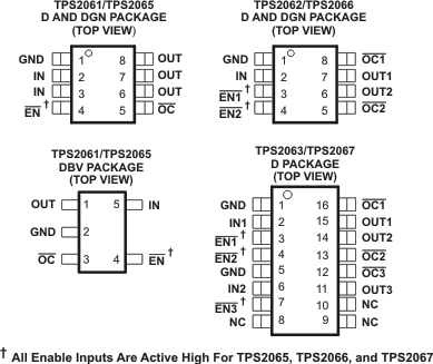
Table 5-1 Pin Functions (TPS2061 and TPS2065)
| PINS | I/O | DESCRIPTION | ||||
|---|---|---|---|---|---|---|
| D or DGN Package | DBV Package | |||||
| NAME | TPS2061 | TPS2065 | TPS2061 | TPS2065 | ||
| EN | 4 | - | 4 | - | I | Enable input, logic low turns on power switch |
| EN | - | 4 | - | 4 | I | Enable input, logic high turns on power switch |
| GND | 1 | 1 | 2 | 2 | Ground | |
| IN | 2, 3 | 2,3 | 5 | 5 | I | Input voltage |
| OC | 5 | 5 | 3 | 3 | O | Overcurrent, open-drain output, active-low |
| OUT | 6, 7, 8 | 6, 7, 8 | 1 | 1 | O | Power-switch output |
| PowerPAD™ | - | - | - | - | Internally connected to GND; used to heat-sink the part to the circuit board traces. Must be connected to GND pin. | |
Table 5-2 Pin Functions (TPS2062 and TPS2066)
| PINS | I/O | DESCRIPTION | ||
|---|---|---|---|---|
| NAME | NO. | |||
| TPS2062 | TPS2066 | |||
| EN1 | 3 | - | I | Enable input, logic low turns on power switch IN-OUT1 |
| EN2 | 4 | - | I | Enable input, logic low turns on power switch IN-OUT2 |
| EN1 | - | 3 | I | Enable input, logic high turns on power switch IN-OUT1 |
| EN2 | - | 4 | I | Enable input, logic high turns on power switch IN-OUT2 |
| GND | 1 | 1 | Ground | |
| IN | 2 | 2 | I | Input voltage |
| OC1 | 8 | 8 | O | Overcurrent, open-drain output, active low, IN-OUT1 |
| OC2 | 5 | 5 | O | Overcurrent, open-drain output, active low, IN-OUT2 |
| OUT1 | 7 | 7 | O | Power-switch output, IN-OUT1 |
| OUT2 | 6 | 6 | O | Power-switch output, IN-OUT2 |
| PowerPAD™ | - | - | Internally connected to GND; used to heat-sink the part to the circuit board traces. Must be connected to GND pin. | |
Table 5-3 Pin Functions (TPS2063 and TPS2067)
| PINS | I/O | DESCRIPTION | ||
|---|---|---|---|---|
| NAME | TPS2063 | TPS2067 | ||
| EN1 | 3 | – | I | Enable input, logic low turns on power switch IN1-OUT1 |
| EN2 | 4 | – | I | Enable input, logic low turns on power switch IN1-OUT2 |
| EN3 | 7 | – | I | Enable input, logic low turns on power switch IN2-OUT3 |
| EN1 | – | 3 | I | Enable input, logic high turns on power switch IN1-OUT1 |
| EN2 | – | 4 | I | Enable input, logic high turns on power switch IN1-OUT2 |
| EN3 | – | 7 | I | Enable input, logic high turns on power switch IN2-OUT3 |
| GND | 1, 5 | 1, 5 | Ground | |
| IN1 | 2 | 2 | I | Input voltage for OUT1 and OUT2 |
| IN2 | 6 | 6 | I | Input voltage for OUT3 |
| NC | 8, 9, 10 | 8, 9, 10 | No connection | |
| OC1 | 16 | 16 | O | Overcurrent, open-drain output, active low, IN1-OUT1 |
| OC2 | 13 | 13 | O | Overcurrent, open-drain output, active low, IN1-OUT2 |
| OC3 | 12 | 12 | O | Overcurrent, open-drain output, active low, IN2-OUT3 |
| OUT1 | 15 | 15 | O | Power-switch output, IN1-OUT1 |
| OUT2 | 14 | 14 | O | Power-switch output, IN1-OUT2 |
| OUT3 | 11 | 11 | O | Power-switch output, IN2-OUT3 |