SLVS496D SEPTEMBER 2003 – August 2016 TPS65100 , TPS65101 , TPS65105
PRODUCTION DATA.
- 1 Features
- 2 Applications
- 3 Description
- 4 Revision History
- 5 Device Options
- 6 Pin Configuration and Functions
- 7 Specifications
- 8 Detailed Description
- 9 Application and Implementation
- 10Power Supply Recommendations
- 11Layout
- 12Device and Documentation Support
- 13Mechanical, Packaging, and Orderable Information
7 Specifications
7.1 Absolute Maximum Ratings
Over operating free-air temperature range (unless otherwise noted)(1)| MIN | MAX | UNIT | |
|---|---|---|---|
| Voltages on pin VIN(2) | –0.3 | 6 | V |
| Voltages on pin SUP, PG (2) | –0.3 | 15.5 | V |
| Voltage on pin FB1, FB2, FB3, FB4 | –0.3 | 5.5 | V |
| Voltages on pin EN, MODE, ENR(2) | –0.3 | VI + 0.3 | V |
| Voltage on VCOMIN | –0.3 | 14 | V |
| Voltage on pin SW(2) | –0.3 | 20 | V |
| Voltage on pin DRV | –0.3 | 15 | V |
| Voltage on pin REF | –0.3 | 4 | V |
| Voltage on pin BASE | –0.3 | 5.5 | V |
| Voltage on pin VOUT3 | –0.3 | 30 | V |
| Voltage on pin VCOM | –0.3 | 15 | V |
| Voltage on pin C1+, C2+ | –0.3 | 30 | V |
| Voltage on pin C1–, C2– | –0.3 | 15 | V |
| Continuous power dissipation | See Dissipation Ratings | ||
| Operating junction temperature, TJ | –40 | 150 | °C |
| Storage temperature, Tstg | –65 | 150 | °C |
(1) Stresses beyond those listed under Absolute Maximum Ratings may cause permanent damage to the device. These are stress ratings only, and functional operation of the device at these or any other conditions beyond those indicated under Recommended Operating Conditions is not implied. Exposure to absolute-maximum-rated conditions for extended periods may affect device reliability.
(2) All voltage values are with respect to network ground terminal.
7.2 ESD Ratings
| VALUE | UNIT | |||
|---|---|---|---|---|
| V(ESD) | Electrostatic discharge | Human-body model (HBM), per ANSI/ESDA/JEDEC JS-001(1) | ±2000 | V |
| Charged-device model (CDM), per JEDEC specification JESD22-C101(2) | ±500 | |||
(1) JEDEC document JEP155 states that 500-V HBM allows safe manufacturing with a standard ESD control process.
(2) JEDEC document JEP157 states that 250-V CDM allows safe manufacturing with a standard ESD control process.
7.3 Recommended Operating Conditions
| MIN | NOM | MAX | UNIT | ||
|---|---|---|---|---|---|
| VI | Input voltage | 2.7 | 5.8 | V | |
| L | Inductor(1) | 4.7 | µH | ||
| TA | Operating free-air temperature | –40 | 85 | °C | |
| TJ | Operating junction temperature | –40 | 125 | °C | |
(1) See the Detailed Design Procedure for further information.
7.4 Thermal Information
| THERMAL METRIC(1) | TPS6510x | UNIT | ||
|---|---|---|---|---|
| PWP (HTSSOP) | RGE (VQFN) | |||
| 24 PINS | 24 PINS | |||
| RθJA | Junction-to-ambient thermal resistance | 37.2 | 33 | °C/W |
| RθJC(top) | Junction-to-case (top) thermal resistance | 18.9 | 35.3 | °C/W |
| RθJB | Junction-to-board thermal resistance | 16.4 | 10.7 | °C/W |
| ψJT | Junction-to-top characterization parameter | 0.4 | 0.4 | °C/W |
| ψJB | Junction-to-board characterization parameter | 16.2 | 10.8 | °C/W |
| RθJC(bot) | Junction-to-case (bottom) thermal resistance | 2.1 | 1.8 | °C/W |
(1) For more information about traditional and new thermal metrics, see the Semiconductor and IC Package Thermal Metrics application report.
7.5 Electrical Characteristics
VI = 3.3 V, EN = VI, VO1 = 10 V, TA = –40°C to 85°C, typical values are at TA = 25°C (unless otherwise noted)| PARAMETER | TEST CONDITIONS | MIN | TYP | MAX | UNIT | |
|---|---|---|---|---|---|---|
| SUPPLY CURRENT | ||||||
| VI | Input voltage range | 2.7 | 5.8 | V | ||
| II(VIN) | Quiescent current (VIN) | ENR = VCOMIN = GND, VO3 = 2 × VO1
Boost converter not switching |
0.7 | 0.9 | mA | |
| II(QCharge) | Charge pump quiescent current (SUP) | VO1 = SUP = 10 V, VO3 = 2 × VO1 | 1.7 | 2.7 | mA | |
| VO1 = SUP = 10 V, VO3 = 3 × VO1 | 3.9 | 6 | ||||
| II(QVCOM) | VCOM quiescent current (SUP) | ENR = GND, VO1 = SUP = 10 V | 750 | 1300 | µA | |
| II(QEN) | LDO controller quiescent current (VIN) | ENR = VI, EN = GND | 300 | 800 | µA | |
| II(sd) | Shutdown current (VIN) | EN = ENR = GND | 1 | 10 | µA | |
| VIT– | Undervoltage lockout threshold | VI falling | 2.2 | 2.4 | V | |
| Thermal shutdown temperature threshold | TJ rising | 160 | °C | |||
| LOGIC SIGNALS | ||||||
| VIH | High-level input voltage (EN, ENR) | 1.5 | V | |||
| VIL | Low-level input voltage (EN, ENR) | 0.4 | V | |||
| IIH , IIL | Input leakage current | EN = ENR = GND or VI | 0.01 | 0.1 | µA | |
| MAIN BOOST CONVERTER VO1 | ||||||
| VO1 | Output voltage range | 5 | 15 | V | ||
| VO1 – VI | Minimum input to output voltage difference |
1 | V | |||
| V(REF) | Reference output voltage (REF) | 1.205 | 1.213 | 1.219 | V | |
| Vref | Feedback regulation voltage (FB1) | 1.136 | 1.146 | 1.154 | V | |
| IIB | Feedback input bias current | 10 | 100 | nA | ||
| rDS(on) | N-MOSFET on-resistance (Q1) | VO1 = 10 V, I(sw) = 500 mA | 195 | 290 | mΩ | |
| VO1 = 5 V, I(sw) = 500 mA | 285 | 420 | ||||
| ILIM | N-MOSFET switch current limit (Q1) | TPS65100, TPS65101 | 1.6 | 2.3 | 2.6 | A |
| TPS65105 | 0.96 | 1.37 | 1.56 | A | ||
| rDS(on) | P-MOSFET on-resistance (Q2) | VO1 = 10 V, I(sw) = 100 mA | 9 | 15 | Ω | |
| VO1 = 5 V, I(sw) = 100 mA | 14 | 22 | ||||
| Maximum P-MOSFET peak switch current | 1 | A | ||||
| I(SW)(off) | Off-state current (SW) | V(sw) = 15 V | 1 | 10 | µA | |
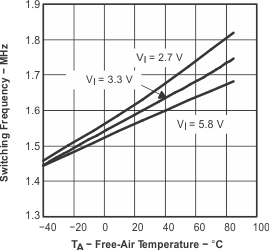
| fOSC | Oscillator frequency | 0°C ≤ TA ≤ 85°C | 1.295 | 1.6 | 2.1 | MHz |
| –40°C ≤ TA ≤ 85°C | 1.191 | 1.6 | 2.1 | |||
| ΔVO(ΔVI) | Line regulation | 2.7 V ≤ VI ≤ 5.7 V, Iload = 100 mA | 0.012 | %/V | ||
| ΔVO(ΔIO) | Load regulation | 0 mA ≤ IO ≤ 300 mA | 0.2 | %/A | ||
| NEGATIVE CHARGE PUMP VO2 | ||||||
| VO2 | Output voltage range | –2 | V | |||
| V(REF) | Reference output voltage (REF) | 1.205 | 1.213 | 1.219 | V | |
| Vref | Feedback regulation voltage (FB2) | –36 | 0 | 36 | mV | |
| IIB | Feedback input bias current | 10 | 100 | nA | ||
| rDS(on) | Q8 P-Channel switch rDS(ON) | IO = 20 mA | 4.3 | 8 | Ω | |
| Q9 N-Channel switch rDS(ON) | 2.9 | 4.4 | ||||
| IOM | Maximum output current | 20 | mA | |||
| ΔVO(ΔVI) | Line regulation | 7 V ≤ VO1 ≤ 15 V, IO = 10 mA, VO2 = –5 V | 0.09 | %/V | ||
| ΔVO(ΔIO) | Load regulation | 1 mA ≤ IO ≤ 20 mA, VO2 = –5 V | 0.126 | %/mA | ||
| POSITIVE CHARGE PUMP VO3 | ||||||
| VO3 | Output voltage range | 30 | V | |||
| V(REF) | Reference output voltage | 1.205 | 1.213 | 1.219 | V | |
| Vref | Feedback regulation voltage (FB3) | 1.187 | 1.214 | 1.238 | V | |
| IIB | Feedback input bias current | 10 | 100 | nA | ||
| rDS(on) | Q3 P-Channel switch rDS(on) | IO = 20 mA | 9.9 | 15.5 | Ω | |
| Q4 N-Channel switch rDS(on) | 1.1 | 1.8 | ||||
| Q5 P-Channel switch rDS(on) | 4.6 | 8.5 | ||||
| Q6 N-Channel switch rDS(on) | 1.2 | 2.2 | ||||
| Vd | D1 – D4 Shottky diode forward voltage | I(D1-D4) = 40 mA | 610 | 720 | mV | |
| IOM | Maximum output current | 20 | mA | |||
| ΔVO(ΔVI) | Line regulation | 10 V ≤ VO1 ≤ 15 V, IO = 10 mA, VO3 = 27 V | 0.56 | %/V | ||
| ΔVO(ΔIO) | Load regulation | 1 mA ≤ IO ≤ 20 mA, VO3 = 27 V | 0.05 | %/mA | ||
| LINEAR REGULATOR CONTROLLER VO4 | ||||||
| VO4 | Output voltage range (FB4) | 4.5 V ≤ VI ≤ 5.5 V, 10 mA ≤ IO ≤ 500 mA | 3.2 | 3.3 | 3.4 | V |
| I(BASE) | Maximum base drive current | VI – VO4 – VBE ≥ 0.5 V (1) | 13.5 | 19 | mA | |
| VI – VO4 – VBE ≥ 0.75 V (1) | 20 | 27 | ||||
| ΔVO(ΔVI) | Line regulation | 4.75 V ≤ VI ≤ 5.5 V, IO = 500 mA | 0.186 | %/V | ||
| ΔVO(ΔIO) | Load regulation | 1 mA ≤ IO ≤ 500 mA, VI = 5 V | 0.064 | %/A | ||
| Start-up current | VO4 ≤ 0.8 V | 11 | 20 | 25 | mA | |
| VCOM BUFFER | ||||||
| Vcm | Common mode input range | 2.25 | VO1-2 | V | ||
| VIo | Input offset voltage (IN) | IO = 0 mA | –25 | 25 | mV | |
| ΔVO(ΔIO) | DC Load regulation | IO = ±25 mA | –30 | 37 | mV | |
| IO = ±50 mA | –45 | 55 | ||||
| IO = ±100 mA | –72 | 85 | ||||
| IO = ±150 mA | –97 | 110 | ||||
| IIB | Input bias current (IN) | –300 | –30 | 300 | nA | |
| IOM | Peak output current | VO1 = 15 V | 1.2 | A | ||
| VO1 = 10 V | 0.65 | A | ||||
| VO1 = 5 V | 0.15 | A | ||||
| FAULT PROTECTION THRESHOLDS | ||||||
| V(th, VO1) | Shutdown threshold | VO1 Rising | –12% VO1 | –8.75% VO1 | –6 VO1 | V |
| V(th, VO2) | VO2 Rising | –13 VO2 | –9% VO2 | –5 VO2 | V | |
| V(th, VO3) | VO3 Rising | –11 VO3 | –8% VO3 | –5 VO3 | V | |
(1) With VI = supply voltage of the TPS6510x, VO4 = output voltage of the regulator, VBE = basis emitter voltage of external transistor
7.6 Dissipation Ratings
| PACKAGE | RΘJA | TA ≤ 25°C POWER RATING |
TA = 70°C POWER RATING |
TA = 85°C POWER RATING |
|---|---|---|---|---|
| 24-Pin TSSOP | 30.13 C°/W (PWP soldered) | 3.3 W | 1.83 W | 1.32 W |
| 24-Pin VQFN | 30 C°/W | 3.3 W | 1.8 W | 1.3 W |
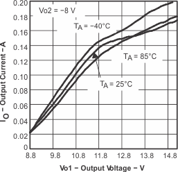
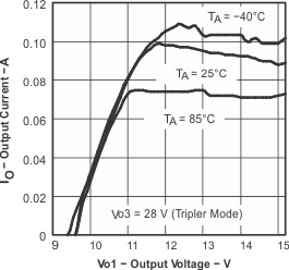
7.7 Typical Characteristics
