SLVS847A November 2008 – December 2016 TPS54917
PRODUCTION DATA.
- 1 Features
- 2 Applications
- 3 Description
- 4 Revision History
- 5 Device Comparison Table
- 6 Pin Configuration and Functions
- 7 Specifications
-
8 Detailed Description
- 8.1 Overview
- 8.2 Functional Block Diagram
- 8.3
Feature Description
- 8.3.1 Undervoltage Lockout (UVLO)
- 8.3.2 Slow Start or Enable (SS/ENA)
- 8.3.3 VBIAS Regulator (VBIAS)
- 8.3.4 Voltage Reference
- 8.3.5 Oscillator and PWM Ramp
- 8.3.6 Error Amplifier
- 8.3.7 PWM Control
- 8.3.8 Dead-Time Control and MOSFET Drivers
- 8.3.9 Overcurrent Protection
- 8.3.10 Thermal Shutdown
- 8.3.11 Power Good (PWRGD)
- 8.4 Device Functional Modes
- 9 Application and Implementation
- 10Power Supply Recommendations
- 11Layout
- 12Device and Documentation Support
- 13Mechanical, Packaging, and Orderable Information
9 Application and Implementation
NOTE
Information in the following applications sections is not part of the TI component specification, and TI does not warrant its accuracy or completeness. TI’s customers are responsible for determining suitability of components for their purposes. Customers should validate and test their design implementation to confirm system functionality.
9.1 Application Information
TPS54917 is a synchronous buck converter. It can convert an input voltage of 3 V to 4 V to a lower voltage. Maximum output current is 9 A.
9.2 Typical Application
Figure 10 shows the schematic diagram for a typical TPS54917 application. The TPS54917 (U1) can provide up to 9 A of output current at a nominal output voltage of 1.8 V. For proper thermal performance, the exposed thermal PowerPAD underneath the integrated circuit (TPS54917) package must be soldered to the printed-circuit board.

9.2.1 Design Requirements
Table 2 lists the design specifications for this application example.
Table 2. Application Circuit Specifications
| PARAMETER | TEST CONDITIONS | MIN | TYP | MAX | UNIT | ||
|---|---|---|---|---|---|---|---|
| INPUT CHARACTERSTICS | |||||||
| VIN | Input voltage | 3 | 3.3 | 4 | V | ||
| OUTPUT CHARACTERSTICS | |||||||
| VOUT | Output voltage 1 | VIN = Nom, IOUT = Nom | 1.8 | V | |||
| IOUT | 0 | 9 | |||||
| TRANSIENT RESPONSE | |||||||
| ΔVOUT | Change from load transient | ΔIOUT = 4.5 A | 50 | mV | |||
| Settling time | to 1% of VOUT | 0.5 | ms | ||||
| SYSTEMS CHARACTERSTICS | |||||||
| fSW | Switching frequency | 1600 | kHz | ||||
9.2.2 Detailed Design Procedure
9.2.2.1 Component Selection
The values for the components used in this design example were selected for best load transient response and small PCB area. Additional design information is available at www.ti.com.
9.2.2.2 Input Filter
The input voltage is a nominal 3.3 VDC. The input filter capacitors (C1 and C2) are 10-µF ceramic capacitors (MuRata). C12 is a 0.01-µF ceramic capacitor that provides high-frequency decoupling of the TPS54917 from the input supply. C1, C2, and C12 must be placed as close as possible to the device. Input ripple current is shared among C1, C2, and C12.
9.2.2.3 Feedback Circuit
The values for these components are selected to provide fast transient response times.
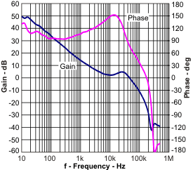
The resistor divider network of R1 and R2 sets the output voltage for the circuit at 1.8 V. R1 along with R6, R7, C5, C7, and C10 forms the loop compensation network for the circuit. For this design, a Type-3 topology is used. The feedback loop is compensated so that the unity gain frequency is approximately 40 kHz.
9.2.2.4 Operating Frequency
In the application circuit, RT is grounded through a 27.4-kΩ resistor to select the operating frequency of 1.6 MHz. To set a different frequency, place a 27-kΩ to 180-kΩ resistor between RT (pin 29) and analog ground or leave RT floating to select the default of 350 kHz. The switching frequency in MHz can be approximated using Equation 4.

9.2.2.5 Output Filter
The output filter is composed of a 0.35-µH inductor and 2 × 100-µF capacitors. The inductor is a dual-coil type (Coilcraft SLC7530-820ML) with the coils wired in series. The capacitors used are 100-µF, 6.3-V ceramic types with X5R dielectric.
9.2.3 Application Curves
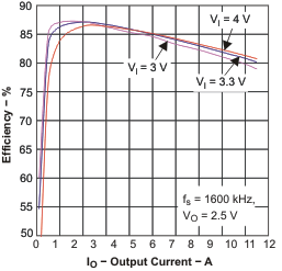
 Figure 11. Efficiency vs Output Current

 Figure 15. Output Ripple Voltage
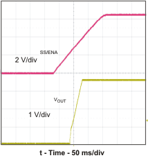
 Figure 17. Slow-Start Timing
 Figure 19. Closed-Loop Response
 Figure 12. Load Regulation vs Output Current

 Figure 16. Transient Response
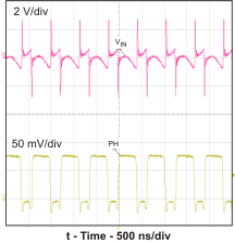
 Figure 18. Input Ripple