SLVS984B September 2009 – March 2015 TPS22946
PRODUCTION DATA.
- 1 Features
- 2 Applications
- 3 Description
- 4 Revision History
- 5 Pin Configuration and Functions
- 6 Specifications
- 7 Parameter Measurement Information
- 8 Detailed Description
- 9 Application and Implementation
- 10Power Supply Recommendations
- 11Layout
- 12Device and Documentation Support
- 13Mechanical, Packaging, and Orderable Information
9 Application and Implementation
NOTE
Information in the following applications sections is not part of the TI component specification, and TI does not warrant its accuracy or completeness. TI’s customers are responsible for determining suitability of components for their purposes. Customers should validate and test their design implementation to confirm system functionality.
9.1 Application Information
9.1.1 On/Off Control
The ON pin controls the state of the switch. Activating ON continuously holds the switch in the on state so long as there is no fault. A junction temperature in excess of 150°C overrides the ON control to turn off the switch. ON is active HIGH and has a low threshold making it capable of interfacing with low voltage signals. When the MOSFET is off, the body diode is disabled so no current can flow through it from the input to the output; however, the body diode does not prevent reverse current flowing.
9.2 Typical Application
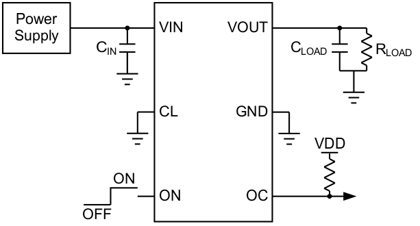
This application demonstrates how the TPS22946 can be used to power a downstream load that includes a capacitive element (CLOAD).
 Figure 34. Typical Application Schematic
9.2.1 Design Requirements
For this design example, use the following as the input parameters.
Table 4. Design Parameters
| DESIGN PARAMETER | EXAMPLE VALUE |
|---|---|
| VIN | 3.3 V |
| Output capacitance (CLOAD) | 1 µF |
| VOUT rise time (tR) | 50 µs |
9.2.2 Detailed Design Procedure
To begin the design process, the designer must know the following:
- VIN voltage
- Output capacitance (CLOAD)
- VOUT rise time (tR)
The TPS22946 has a 435-mA current limit during initial turnon of the switch, Ilimit_inrush. This current limit is higher than the steady-state current limit, ILIM. The purpose of this feature is to allow the inrush current that is caused by charging up the capacitor, CLOAD. To calculate the inrush current that is caused by the capacitor during initial turnon, use the following equation:

where
- IINRUSH = amount of inrush current caused by CLOAD
- CL = capacitance on VOUT
- dt = VOUT rise time
- dVOUT = increase in VOUT during the rise time
Using the given example values, the inrush current in this typical application will be 66-mA:
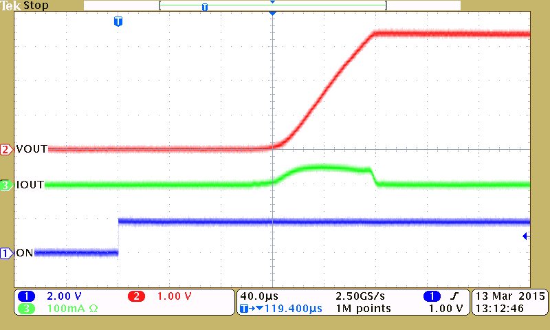
The oscilloscope capture in Figure 35 shows the inrush current for the given design example.
9.2.3 Application Curve
 Figure 35. Inrush Current With 1-µF Output Capacitor