TPS6102x 96% Efficient Synchronous Boost Converters
1 Features
- Qualified for Automotive Applications
- 96% Efficient Synchronous Boost Converter
- Output Voltage Remains Regulated When Input Voltage Exceeds Nominal Output Voltage
- Device Quiescent Current: 25 µA (Typ)
- Input Voltage Range: 0.9 V to 6.5 V
- Fixed and Adjustable Output Voltage Options Up to 5.5 V
- Power Save Mode for Improved Efficiency at Low Output Power
- Low Battery Comparator
- Low EMI-Converter (Integrated Anti-ringing Switch)
- Load Disconnect During Shutdown
- Over-Temperature Protection
- Small 3-mm × 3-mm QFN-10 Package
2 Applications
- All One-Cell, Two-Cell and Three-Cell Alkaline, NiCd or NiMH or Single-Cell Li Battery Powered Products
- Portable Audio Players
- PDAs
- Cellular Phones
- Personal Medical Products
- Camera White LED Flash Light
3 Description
The TPS6102x devices provide a power supply solution for products powered by either a one-cell, two-cell, or three-cell alkaline, NiCd or NiMH, or one-cell Li-Ion or Li-polymer battery. Output currents can go as high as 200 mA while using a single-cell alkaline, and discharge it down to 0.9 V. It can also be used for generating 5 V at 500 mA from a 3.3-V rail or a Li-Ion battery. The boost converter is based on a fixed frequency, pulse-width-modulation (PWM) controller using a synchronous rectifier to obtain maximum efficiency. At low load currents, the converter enters the Power Save Mode to maintain a high efficiency over a wide load current range. The Power Save Mode can be disabled, forcing the converter to operate at a fixed switching frequency. The maximum peak current in the boost switch is limited to a value of 800 mA, 1500 mA or 1800 mA depending on the device version.
The TPS6102x devices keep the output voltage regulated even when the input voltage exceeds the nominal output voltage. The output voltage can be programmed by an external resistor divider, or is fixed internally on the chip. The converter can be disabled to minimize battery drain. During shutdown, the load is completely disconnected from the battery. A low-EMI mode is implemented to reduce ringing and, in effect, lower radiated electromagnetic energy when the converter enters the discontinuous conduction mode. The device is packaged in a 10-pin VSON PowerPAD™ package.
Device Information(1)
| PART NUMBER | PACKAGE | BODY SIZE (NOM) |
|---|---|---|
| TPS61025-Q1 | VSON (10) | 3.00mm x 3.00mm |
| TPS61027-Q1 | ||
| TPS61029-Q1 |
- For all available packages, see the orderable addendum at the end of the datasheet.
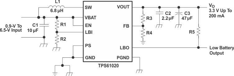
4 Simplified Schematic
5 Revision History
Changes from * Revision (November 2009) to A Revision
- Added Device Information table, Feature Description section, Device Functional Modes, Application and Implementation section, Power Supply Recommendations section, Layout section, Device and Documentation Support section, and Mechanical, Packaging, and Orderable Information section Go
- Added ESD Ratings table Go
- Improved image quality for all equations and figures.Go
6 Device Comparison Table
| PART NUMBER (1) | OUTPUT VOLTAGE (DC/DC) | NOMINAL SWITCH CURRENT LIMIT |
|---|---|---|
| TPS61029-Q1 | Adjustable | 1800 mA |
| TPS61025-Q1(2) | 3.3 V | 1500 mA |
| TPS61027-Q1(2) | 5 V | 1500 mA |
7 Pin Configuration and Functions
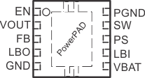
Pin Functions
| PIN | I/O | DESCRIPTION | |
|---|---|---|---|
| NAME | NO. | ||
| EN | 1 | I | Enable input (1/VBAT enabled, 0/GND disabled) |
| FB | 3 | I | Voltage feedback of adjustable versions |
| GND | 5 | Control / logic ground | |
| LBI | 7 | I | Low battery comparator input (comparator enabled with EN), may not be left floating, should be connected to GND or VBAT if comparator is not used |
| LBO | 4 | O | Low battery comparator output (open drain) |
| PS | 8 | I | Enable/disable power save mode (1/VBAT disabled, 0/GND enabled) |
| SW | 9 | I | Boost and rectifying switch input |
| PGND | 10 | Power ground | |
| VBAT | 6 | I | Supply voltage |
| VOUT | 2 | O | Boost converter output |
| PowerPAD™ | Must be soldered to achieve appropriate power dissipation. Should be connected to PGND. | ||