SLVSAI0J October 2010 – May 2016 TPS82670 , TPS826711 , TPS826716 , TPS82672 , TPS826721 , TPS82673 , TPS82674 , TPS826745 , TPS82676 , TPS826765 , TPS82677
UNLESS OTHERWISE NOTED, this document contains PRODUCTION DATA.
- 1 Features
- 2 Applications
- 3 Description
- 4 Simplified Schematic
- 5 Revision History
- 6 Device Comparison Table
- 7 Pin Configuration and Functions
- 8 Specifications
- 9 Detailed Description
- 10Applications and Implementation
- 11Power Supply Recommendations
- 12Layout
- 13Device and Documentation Support
- 14Mechanical, Packaging, and Orderable Information
8 Specifications
8.1 Absolute Maximum Ratings
over operating free-air temperature range (unless otherwise noted)(1)| MIN | MAX | UNIT | |||
|---|---|---|---|---|---|
| VI (3) | Voltage at VIN(2) | –0.3 | 6 | V | |
| Voltage at VIN (TPS826721)(2) | -0.3 | 5.5 | |||
| Voltage at VOUT | –0.3 | 3.6 | V | ||
| Voltage at EN, MODE | –0.3 | VIN + 0.3 | V | ||
| Power dissipation | Internally limited | ||||
| TA | Operating temperature range(4) | –40 | 85 | °C | |
| TINT (max) | Maximum internal operating temperature | 125 | °C | ||
| Tstg | Storage temperature | –55 | 125 | °C | |
(1) Stresses beyond those listed under absolute maximum ratings may cause permanent damage to the device. These are stress ratings only and functional operation of the device at these or any other conditions beyond those indicated under recommended operating conditions is not implied. Exposure to absolute-maximum-rated conditions for extended periods may affect device reliability.
(2) Operation above 4.8V input voltage for extended periods may affect device reliability.
(3) All voltage values are with respect to network ground terminal.
(4) In applications where high power dissipation and/or poor package thermal resistance is present, the maximum ambient temperature may have to be derated. Maximum ambient temperature (TA(max)) is dependent on the maximum operating temperature (TINT(max)), the maximum power dissipation of the device in the application (PD(max)), and the junction-to-ambient thermal resistance of the part/package in the application (RθJA), as given by the following equation: TA(max)= TJ(max)–(RθJA X PD(max)). To achieve optimum performance, it is recommended to operate the device with a maximum internal temperature of 105°C.
8.2 ESD Ratings
| VALUE | UNIT | ||
|---|---|---|---|
| VESD(1) | Human body model (HBM) ESD stress voltage(2) | ±2000 | V |
| Charge device model (CDM) ESD stress voltage(3) | ±1000 | ||
| Machine model (MM) ESD stress voltage(4) | ±200 | V | |
(1) Electrostatic discharge (ESD) to measure device sensitivity and immunity to damage caused by assembly line electrostatic discharges in to the device.
(2) Level listed above is the passing level per ANSI, ESDA, and JEDEC JS-001. JEDEC document JEP155 states that 500-V HBM allows safe manufacturing with a standard ESD control process.
(3) Level listed above is the passing level per EIA-JEDEC JESD22-C101. JEDEC document JEP157 states that 250-V CDM allows safe manufacturing with a standard ESD control process.
(4) The machine model is a 200-pF capacitor discharged directly into each pin.
8.3 Recommended Operating Conditions
over operating free-air temperature range (unless otherwise noted)| MIN | NOM | MAX | UNIT | |||
|---|---|---|---|---|---|---|
| VIN | Input voltage range | 2.3 | 4.8(2) | V | ||
| IO | Output current range | TPS82671 to TPS826765 | 0 | 600 | mA | |
| Additional output capacitance (PFM/PWM operation)(1) | TPS82670 to TPS82676 TPS826711, TPS826716, TPS826721, TPS826765, TPS8267195 |
0 | 2.5 | µF | ||
| TPS82677 | 0 | 4 | µF | |||
| Additional output capacitance (PWM operation)(1) | 0 | 7 | µF | |||
| TA | Ambient temperature | –40 | +85 | °C | ||
| TJ | Operating junction temperature | –40 | +125 | °C | ||
(1) In certain applications larger capacitor values can be tolerable, see Output Capacitor Selection section for more details.
8.4 Thermal Information
| THERMAL METRIC(1) | TPS8267x | UNIT | |
|---|---|---|---|
| SIP | |||
| 8 PINS | |||
| RθJA | Junction-to-ambient (top) thermal resistance | 125 | °C/W |
| Junction-to-ambient (bottom) thermal resistance | 70 | ||
| RθJCtop | Junction-to-case (top) thermal resistance | - | |
| RθJB | Junction-to-board thermal resistance | - | |
| ψJT | Junction-to-top characterization parameter | - | |
| ψJB | Junction-to-board characterization parameter | - | |
| RθJCbot | Junction-to-case (bottom) thermal resistance | - | |
(1) For more information about traditional and new thermal metrics, see the IC Package Thermal Metrics application report, SPRA953.
8.5 Electrical Characteristics
Minimum and maximum values are at VIN = 2.3V to 5.5V, VOUT = 1.8V, EN = 1.8V, AUTO mode and TA = –40°C to 85°C; Circuit of Parameter Measurement Information section (unless otherwise noted). Typical values are at VIN = 3.6V, VOUT = 1.8V, EN = 1.8V, AUTO mode and TA = 25°C (unless otherwise noted).8.6 Typical Characteristics
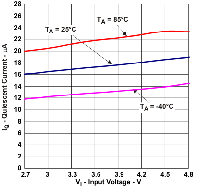
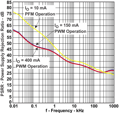
| VI = 3.6 V | VO = 1.8 V | (TPS82671) |
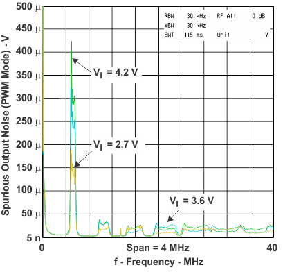
| VO = 1.8 V | RL = 12 Ω | (TPS82671) |
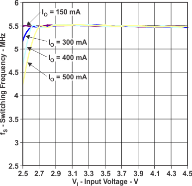
| VO = 1.8 V |
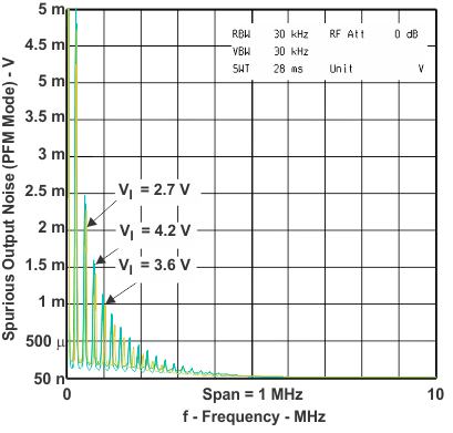
| VO = 1.8 V | RL = 150 Ω | (TPS82671) |
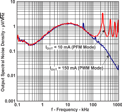
| VI = 3.6 V | VO = 1.8 V | (TPS82671) |