SLVSB16E November 2011 – December 2015 TPS43340-Q1
PRODUCTION DATA.
- 1 Features
- 2 Applications
- 3 Description
- 4 Revision History
- 5 Pin Configuration and Functions
- 6 Specifications
-
7 Detailed Description
- 7.1 Overview
- 7.2 Functional Block Diagram
- 7.3 Feature Description
- 7.4 Device Functional Modes
- 8 Application and Implementation
- 9 Power Supply Recommendations
- 10Layout
- 11Device and Documentation Support
- 12Mechanical, Packaging, and Orderable Information
8 Application and Implementation
NOTE
Information in the following applications sections is not part of the TI component specification, and TI does not warrant its accuracy or completeness. TI’s customers are responsible for determining suitability of components for their purposes. Customers should validate and test their design implementation to confirm system functionality.
8.1 Application Information
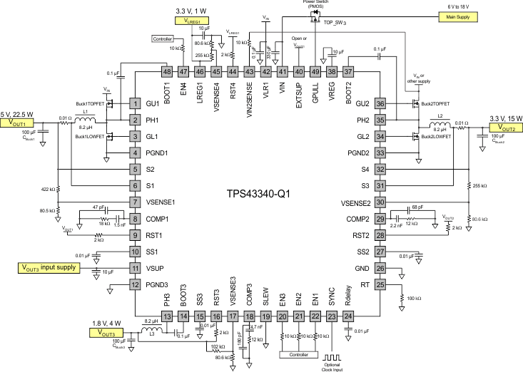
The TPS43340-Q1 multirail power supply operates with a supply voltage VIN of 4 V to 40 V for the Buck controllers and the LDO. The TPS43340-Q1 Buck converter (Buck3) operates with a supply voltage VSUP of 4 V to 10 V. For reducing power dissipation, TI strongly recommends using the output voltage of one of the buck regulators as the input supply for the LDO regulator. To use the output voltage of the buck regulator this way, the selected buck-regulator output voltage must be higher than the selected LDO-regulator output voltage. For further efficiency improvements, the part offers a pin to control an external FET that can bypass the reverse-polarity-protection diode (GPULL).
8.2 Typical Application

8.2.1 Design Requirements
A few parameters must be known to begin the design process. Determination of these parameters is typically at the system level.
The following example illustrates the design process and component selection for the TPS43340-Q1. Table 1 lists the design goal parameters.
Table 1. Application Example
| PARAMETER | Buck1 | Buck2 | Buck3 |
|---|---|---|---|
| Input voltage, VIN | 6 V to 18 V 14 V, typical |
6 V to 18 V 14 V, typical |
4 V to 10 V 5 V, typical |
| Output ripple voltage | ±0.2 V | ±0.2 V | ±0.1 V |
| Output voltage, VOUT | 5 V ±2% | 3.3 V ±2% | 1.8 V ±2% |
| Maximum output current, IOUT | 4.5 A | 4.5 A | 2.2 A |
| Minimum output current, IOUT | 0.1 A | 0.1 A | 0.1 A |
| Load-step output tolerance, ∆VOUT + ∆VOUT(Ripple) | ±0.3 V | ±0.3 V | ±0.15 V |
| Current-output load step, ∆IOUT | 0.1 A to 4.5 A | 0.1 A to 4.5 A | 0.1 A to 2.2 A |
| Converter switching frequency, fSW | 400 kHz | 400 kHz | 400 kHz |
| Junction temperature, TJ | 125°C | 125°C | 125°C |
8.2.2 Detailed Design Procedure
8.2.2.1 High- and Low-Side Power NMOS Selection for the Buck Converters
An internal supply, which is 5.8 V typical under normal operating conditions, provides the gate-drive supply for these MOSFETs. The output is a totem pole, allowing full voltage drive of VREG to the gate with a peak output current of 0.6 A. The high-side MOSFET reference is the phase terminal (PHx), and the low-side MOSFET referenced is the power ground (PGNDx) terminal. For a particular application, select these MOSFETs with consideration for the following parameters rDS(on), gate charge Qg, drain-to-source breakdown voltage BVDSS, maximum dc current IDC(maximum), and thermal resistance for the package.
Power dissipation on the high-side FET (PD_HS):

First term is conduction losses.
Second term is switching losses.
Power dissipation on the low-side FET (PD_LS):

The first term in the foregoing equation refers to conduction losses, and the second term covers the switching losses in the FET body diode during the dead-time.
NOTE
rDS(on) has a positive temperature coefficient TC, which is typically 0.4%/°C.
Gate losses for high-side and low-side FETs:
8.2.2.2 Buck1 Component Selection

Selection of Current Sensing Resistor

Use 10 mΩ to allow for ripple-current.
Inductor Selection L

Use 8.2 µH.
Inductor Ripple Current
Output Capacitor COUT
Use 100 µF.

Input Capacitor CIN
Use 10 µF, shared between Buck1 and Buck2.
High-Side MOSFET (Buck1TOPFET)
Low-Side MOSFET (Buck1LOWFET)
8.2.2.3 Buck2 Component Selection
Selection of Current-Sensing Resistor

Use 10 mΩ to allow for ripple current.
Inductor Selection L

Use 8.2 uH.
Inductor Ripple Current
Output Capacitor COUT
Use 100 µF.

Input Capacitor CIN
Use 10 µF, shared between Buck1 and Buck2. For better line-transient immunity, use a larger value.
High-Side MOSFET (Buck2TOPFET)
Low-Side MOSFET (Buck2LOWFET)

8.2.2.4 Buck3 Component Selection
Inductor Selection LBuck3

Use 8.2 µH.
Inductor Ripple Current
Output Capacitor COUT
Use 100 µF.
Input Capacitor CIN
Use 10 µF.

Internal High-Side MOSFET (Buck3TOPFET)

Internal Low-Side MOSFET (Buck3LOWFET)

8.2.3 Application Curves
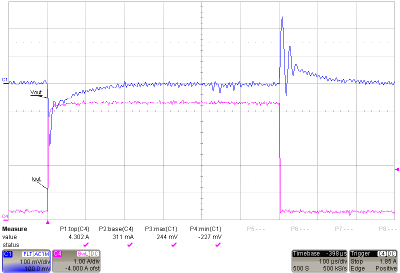
 Figure 21. Load Step Buck 1
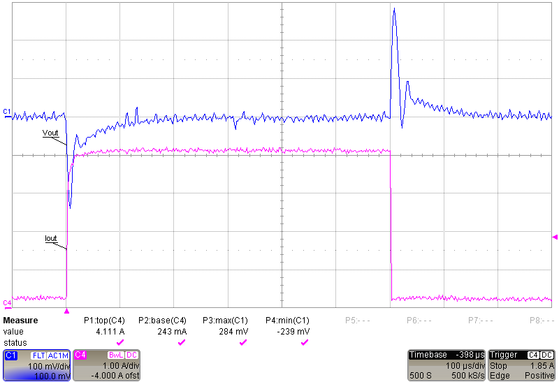
 Figure 23. Load Step Buck 3
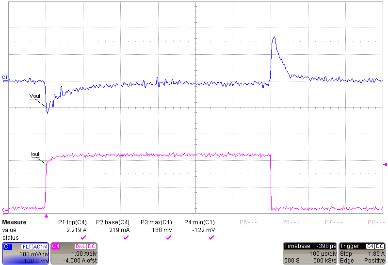
 Figure 22. Load Step Buck 2


