TPS6273x Programmable Output Voltage Ultra-Low Power Buck Converter With Up to 50 mA / 200 mA Output Current
1 Features
- Industry's Highest Efficiency at Low Output Currents: > 90% With IOUT = 15 µA
-
Ultra-Low Power Buck Converter
- TPS62736 Optimized for 50-mA Output Current
- TPS62737 Optimized for 200-mA Output Current
- 1.3-V to 5-V Resistor Programmable Output Voltage Range
- 2-V to 5.5-V Input Operating Range
- 380-nA and 375-nA Quiescent Current During Active Operation for TPS62736 and TPS62737
- 10-nA Quiescent Current During Ship Mode Operation
- 2% Voltage Regulation Accuracy
- 100% Duty Cycle (Pass Mode)
- EN1 and EN2 Control
- Two Power-Off States:
- Shipmode (Full Power-Off State)
- Standby Mode Includes VIN_OK Indication
- Two Power-Off States:
- Input Power-Good Indication (VIN_OK)
- Push-Pull Driver
- Resistor Programmable Threshold Level
2 Applications
- Ultra-Low Power Applications
- 2-Cell and 3-Cell Alkaline-Powered Applications
- Energy Harvesting
- Solar Chargers
- Thermal Electric Generator (TEG) Harvesting
- Wireless Sensor Networks (WSN)
- Low-Power Wireless Monitoring
- Environmental Monitoring
- Bridge and Structural Health Monitoring (SHM)
- Smart Building Controls
- Portable and Wearable Health Devices
- Entertainment System Remote Controls
3 Description
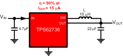
The TPS6273x family provides a highly integrated ultra low power buck converter solution that is well suited for meeting the special needs of ultra-low power applications such as energy harvesting. The TPS6273x provides the system with an externally programmable regulated supply to preserve the overall efficiency of the power-management stage compared to a linear step-down converter. This regulator is intended to step-down the voltage from an energy storage element such as a battery or super capacitor to supply the rail to low-voltage electronics. The regulated output has been optimized to provide high efficiency across low-output currents (<10 µA) to high currents (200 mA).
The TPS6273x integrates an optimized hysteretic controller for low-power applications. The internal circuitry uses a time-based sampling system to reduce the average quiescent current.
Device Information(1)
| PART NUMBER | PACKAGE | BODY SIZE (NOM) |
|---|---|---|
| TPS6273x | VQFN (14) | 3.50 mm × 3.50 mm |
- For all available packages, see the orderable addendum at the end of the datasheet.
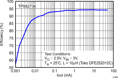
Efficiency vs Output Current
4 Revision History
Changes from B Revision (July 2013) to C Revision
- Added ESD Ratings table, Feature Description section, Device Functional Modes, Application and Implementation section, Power Supply Recommendations section, Layout section, Device and Documentation Support section, and Mechanical, Packaging, and Orderable Information section. Go
Changes from A Revision (March 2013) to B Revision
- Added the TPS62737 Pinout informationGo
- Added graphs for TPS62737 to the Typical CharacteristicsGo
- Added the TPS62737 Application Circuit.Go
- Changed Figure 72Go
- Added Figure 73Go
Changes from * Revision (October 2012) to A Revision
- Changed the device From: Preview To: ActiveGo
5 Description (continued)
To further assist users in the strict management of their energy budgets, the TPS6273x toggles the input power-good indicator to signal an attached microprocessor when the voltage on the input supply has dropped below a preset critical level. This signal is intended to trigger the reduction of load currents to prevent the system from entering an undervoltage condition. In addition, independent enable signals allow the system to control whether the converter is regulating the output, monitoring only the input voltage, or to shut down in an ultra-low quiescent sleep state.
The input power-good threshold and output regulator levels are programmed independently through external resistors.
All the capabilities of TPS6273x are packed into a small footprint 14-lead 3.5-mm × 3.5-mm QFN package (RGY).