SLVSDZ4D February 2018 – February 2020 TPS2HB35-Q1
PRODUCTION DATA.
- 1 Features
- 2 Applications
- 3 Description
- 4 Revision History
- 5 Device Comparison Table
- 6 Pin Configuration and Functions
- 7 Specifications
- 8 Parameter Measurement Information
-
9 Detailed Description
- 9.1 Overview
- 9.2 Functional Block Diagram
- 9.3
Feature Description
- 9.3.1 Protection Mechanisms
- 9.3.2 Diagnostic Mechanisms
- 9.4 Device Functional Modes
- 10Application and Implementation
- 11Power Supply Recommendations
- 12Layout
- 13Device and Documentation Support
- 14Mechanical, Packaging, and Orderable Information
10.1 Application Information
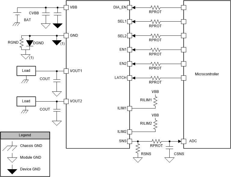
Figure 50 shows the schematic of a typical application for the TPS2HB35-Q1. It includes all standard external components. This section of the datasheet discusses the considerations in implementing commonly required application functionality.

With the ground protection network, the device ground will be offset relative to the microcontroller ground.
Figure 50. System Diagram Table 12. Recommended External Components
| COMPONENT | TYPICAL VALUE | PURPOSE |
|---|---|---|
| RPROT | 15 kΩ | Protect the microcontroller and device I/O pins. |
| RSNS | 1 kΩ | Translate the sense current into sense voltage. |
| CSNS | 100 pF - 10 nF | Creates Low-pass filter for the ADC input |
| RGND | 4.7 kΩ | Stabilize GND potential during turn-off of inductive load. |
| DGND | BAS21 Diode | Protect the device during reverse battery. |
| RILIM | 5 kΩ - 25 kΩ | Set the current limit threshold. |
| CVBB | 4.7 nF to Device GND | Filters voltage transients (for example, ESD, ISO7637-2) and improves emissions |
| 220 nF to Module GND | Stabilize the input supply and filter out low frequency noise. | |
| COUT | 220 nF | Filters voltage transients (for example, ESD, ISO7637-2) |