SLVT208 April 2024 TPS22995H-Q1
Power-supply sequencing becomes an important factor when designing for complex electronics devices which operate from multiple voltage rails, such as Microcontrollers, Microprocessors, FPGAs, ADCs, and so forth. More importantly, in automotive applications, especially those in infotainment and ADAS, the microprocessors require power sequences with different timing configurations and ramp rates. This means the multiple rails power up and power down in various orders with varying capacitances and loading condition, so both turn on order and slew rate matter. The rails sequencing order and slew rate make sure that the internal circuitry is properly biased and staggers the in-rush current at start-up stage. Therefore, the use of electronic ICs with adjustable slew rate option is advantageous for above mentioned applications.
Among available options, load switches are a great potion for power sequencing in designs because load switches provide flexibility and increased protection in a smaller design size. Load switches offer design flexibility and simple control of subsystem power sequencing. Each rail can turn on and off independently without extensive processor intervention, and the rise and fall time of each rail is adjustable. This is possible because of features available in integrated load switches such as configurable rise time and fall time using an external resistance (RT) and quick output discharge (QOD) internal or external to the IC. The TPS22995H-Q1 is an example of an integrated load switch that has both of these features available.
For automotive applications (with specific power sequencing requirements) integrated or discrete load switch can be used. All integrated load switches connect the gate of the internal FET to an external pin for slew rate control. Normally this is not a concern, but with a high humidity environment, up to 100kΩ can be connected from the gate to GND. This overwhelms the charge pump and prevents the load switch from turning on. For a situation like this where integrated load switch fails on the system due to high humidity, system designers usually choose a discrete load switch. A discrete design does not rely on a charge pump and can therefore overpower a 100kΩ short to GND. However, this is normally not preferred because the bill of materials (BOM) count, cost, and design size increase. Choose a functional design with optimized BOM cost and footprint. The TPS22995H-Q1 is the first automotive load switch to provide adjustable slew rate control with humidity resistance. Compared to discrete designs, TPS22995H-Q1 is smaller in size and offers lower BOM count.
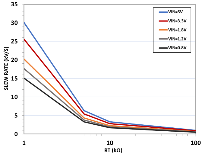
Figure 1 shows the TPS22995H-Q1 IC pinout and functional diagram. The RT resistor can be used as an external component to adjust the slew rate. Increasing RT reduces the slew rate of VOUT ramp.
 Figure 1 TPS22995H-Q1 IC Pinout and
Functional Diagram
Figure 1 TPS22995H-Q1 IC Pinout and
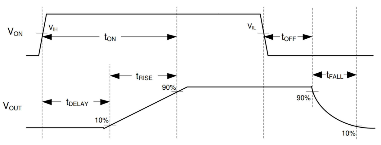
Functional DiagramFigure 3 shows the Timing Diagram for Rise and Fall Time and Slew Rate Measurement. Changing the RT value has a direct impact on the time elapsed from 10% to 90% of the VOUT during rising edge. For a faster tRISE, one has to decrease the RT value. Contrarily, to slow down the rise time, larger RT must be used.
 Figure 2 Timing Diagram for Rise and Fall
Time and Slew Rate Measurement
Figure 2 Timing Diagram for Rise and Fall
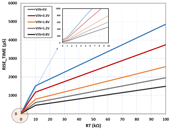
Time and Slew Rate MeasurementFor applications where a specific VOUT ramp rate is required, the designer can achieve this by choosing a larger or smaller RT resistance, as shown in the graphs in Figure 3 and Figure 4.
 Figure 3 TPS22995H-Q1 Rise Time vs
RT
 Figure 4 TPS22995H-Q1 Slew Rate vs
RT
Figure 4 TPS22995H-Q1 Slew Rate vs
RTConclusions
Integrated load switches are an effective plan for electronic applications with specific requirements for power sequencing and controlled rise time, while maintaining lower BOM count and smaller PCB area on the system. However, using these devices under extreme operating condition such as high humidity environment becomes a major engineering challenge. As discussed in this article, TPS22995H-Q1 increases circuit robustness by integrating tolerance to high humidity environments. This humidity feature allows the device to continue functioning as expected, meeting the design goal. Additionally, if the device experiences a 100kΩ short from any pin to GND or power, the device continues to function normally. Therefore, with increasing demand for fault-tolerant ICs with lower BOM cost and footprint, the TI TPS22995H-Q1 offers an excellent choice and removes concerns in the design.