SLVU097B October 2003 – October 2021 TPS54350
3.1 Layout
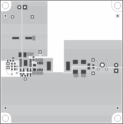
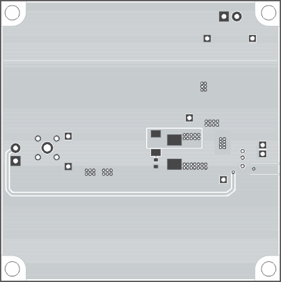
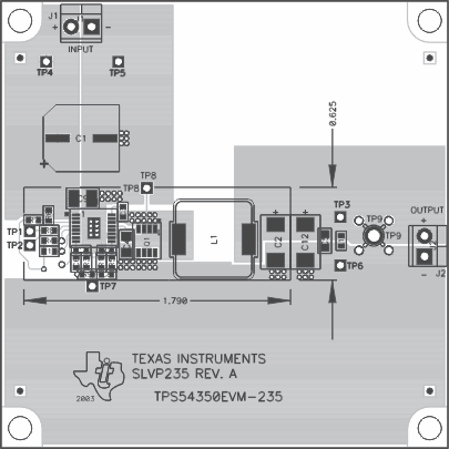
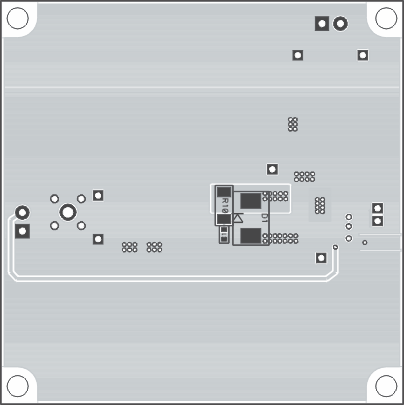
Theboard layout for the TPS54350EVM−235 is shown in Figure 3−1 through Figure 3−4. The topside layer of the TPS54350EVM−235 is laid out in a manner typical of a user application that is optimized for small size. The top and bottom layers are 1.5 oz. copper.
The top layer contains the main power traces for VI, VO, and Vphase. Also, on thetop layer are connections for the remaining pins of the TPS54350 and a large area filled with ground. The bottom layer consists of a ground plane along with aVphase area and the Vsense trace. The bottom layer also has pads for placing snubber components (R10 and C11) and an optional catch diode (D1). The top and bottom ground traces are connected with multiple vias placed around the board including 8 directly under the TPS54350 device to provide a thermal path from the PowerPADä landto ground.
The input decoupling capacitor (C9), bias decoupling capacitor (C4), andbootstrap capacitor (C3) are all located as close to the IC as possible. In addition, the compensation components are also kept close to the IC. The compensation circuit ties to the output voltage at the point of regulation, at the positive output connection.
 Figure 3-1 Top Side Layout
 Figure 3-2 Bottom Side Layout
 Figure 3-3 Top Side Assmebly
 Figure 3-4 Bottom Side Assmebly