SLVU487A October 2011 – October 2021 TPS54329E
4.9 Start-Up
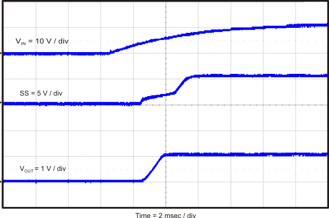
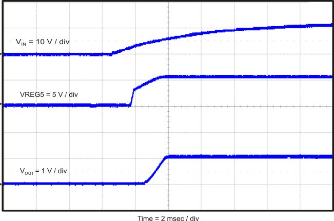
Figure 4-11 and Figure 4-12 show the TPS54329EEVM-056 start-up waveforms relative to VIN.
 Figure 4-11 TPS54329EEVM-056 Start-Up Relative to VIN With SS
 Figure 4-12 TPS54329EEVM-056 Start-Up Relative to VIN With VREG5
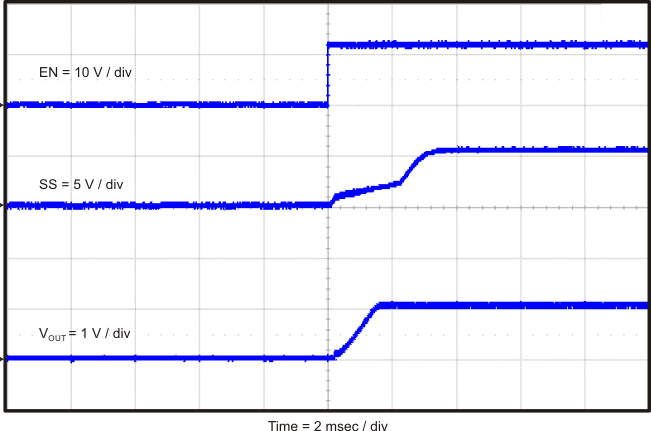
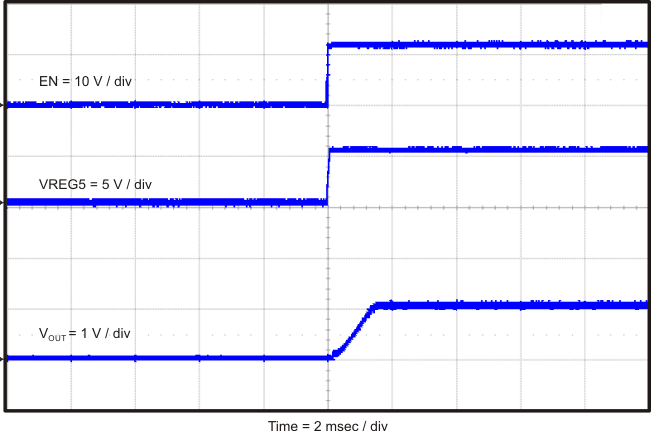
Figure 4-13 and Figure 4-14 show the TPS54329EEVM-056 start-up waveforms relative to enable (EN).
 Figure 4-13 TPS54329EEVM-056 Start-Up Relative to EN With SS
 Figure 4-14 TPS54329EEVM-056 Start-Up Relative to EN With VREG5