SLVU745A August   2012  – May 2021 TPS54495


  1.   Trademarks
  2. 1Introduction
  3. 2Performance Specification Summary
  4. 3Modifications
    1. 3.1 Output Voltage Setpoint
    2. 3.2 Output Filter and Closed-Loop Response
  5. 4Test Setup and Results
    1. 4.1 Input/Output Connections
    2. 4.2 Start-Up Procedure
    3. 4.3 Efficiency
      1. 4.3.1 Efficiency of Converter 1
      2. 4.3.2 Efficiency of Converter 2
    4. 4.4 Load Regulation
      1. 4.4.1 Load Regulation of Converter 1
      2. 4.4.2 Load Regulation of Converter 2
    5. 4.5 Line Regulation
      1. 4.5.1 Line Regulation Converter 1
      2. 4.5.2 Line Regulation Converter 2
    6. 4.6 Load Transient Response
      1. 4.6.1 Load Transient Response Converter 1
      2. 4.6.2 Load Transient Response Converter 2
    7. 4.7 Output Voltage Ripple
      1. 4.7.1 Output Voltage Ripple Converter 1
      2. 4.7.2 Output Voltage Ripple Converter 2
    8. 4.8 Input Voltage Ripple
    9. 4.9 Start-Up
      1. 4.9.1 Converter 1 Start-Up
      2. 4.9.2 Converter 2 Start-Up
  6. 5Board Layout
    1. 5.1 Layout
  7. 6Schematic, Bill of Materials, and Reference
    1. 6.1 Schematic
    2. 6.2 Bill of Materials
    3. 6.3 Reference
  8. 7Revision History

Schematic

Figure 6-1 is the schematic for the TPS54495EVM.
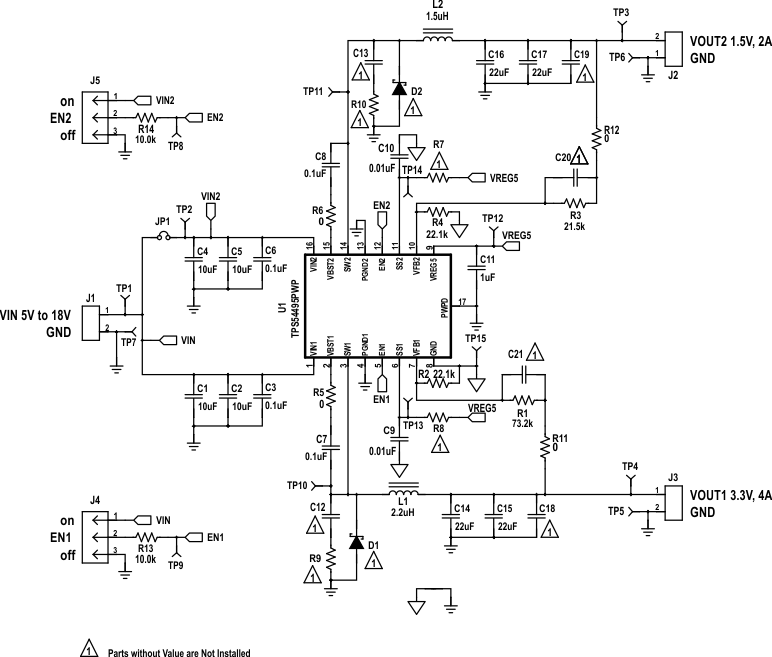
GUID-89BA5C28-F1C9-43D1-9933-FCEE1A4E788A-low.gifFigure 6-1 TPS54495EVM Schematic Diagram