SLVU814A November   2012  – October 2021 TPS54339E


  1.   Trademarks
  2. 1Introduction
  3. 2Performance Specification Summary
  4. 3Modifications
    1. 3.1 Output Voltage Setpoint
    2. 3.2 Output Filter and Closed-Loop Response
  5. 4Test Setup and Results
    1. 4.1  Input/Output Connections
    2. 4.2  Start-Up Procedure
    3. 4.3  Efficiency
    4. 4.4  Load Regulation
    5. 4.5  Line Regulation
    6. 4.6  Closed Loop Response
    7. 4.7  Load Transient Response
    8. 4.8  Output Voltage Ripple
    9. 4.9  Input Voltage Ripple
    10. 4.10 Start-Up
    11. 4.11 Shut-Down
  6. 5Board Layout
    1. 5.1 Layout
  7. 6Schematic, Bill of Materials, and Reference
    1. 6.1 Schematic
    2. 6.2 Bill of Materials
    3. 6.3 Reference
  8. 7Revision History

Schematic

Figure 6-1 is the schematic for the TPS54339EEVM-056.
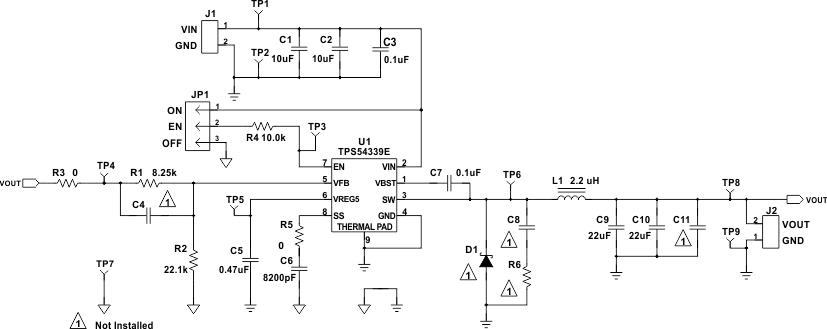
GUID-E6BFC8BA-9288-4BB1-8DB5-AF7D82BE8B0B-low.gifFigure 6-1 TPS54339EEVM-056 Schematic Diagram