SLVU892A March 2013 – June 2021 TPS56428
5.1 Layout
The board layout for the TPS56428EVM-534 is shown in Figure 5-1 through Figure 5-5. The top layer contains the main power traces for VIN, VOUT, and ground. Also on the top layer are connections for the pins of the TPS56428 and a large area filled with ground. Many of the signal traces also are located on the top side. The input decoupling capacitors are located as close to the IC as possible. The input and output connectors, test points, and all of the components are located on the top side. Internal layer 1, Internal layer 2 and the bottom layer are predominantly power ground planes. An analog ground (AGND) area is provided on internal layer 1. Analog ground (AGND) and power ground (PGND) are connected at a single point on the internal layer 1 as shown. Internal layer 2 contains an additional VIN area as well as a connection to the VIN pin of the EN control jumper JP1. The bottom layer contains the output voltage feedback trace.
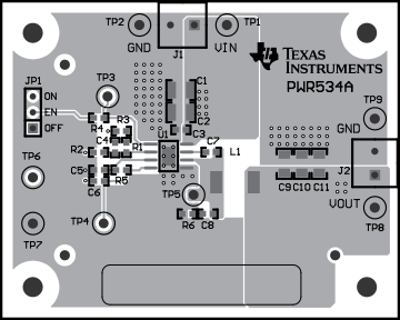 Figure 5-1 Top Assembly
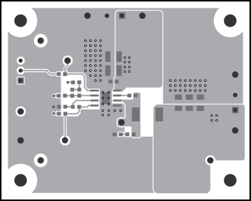 Figure 5-2 Top Layer
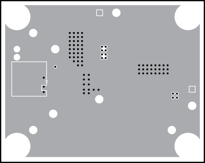 Figure 5-3 Internal Layer 1
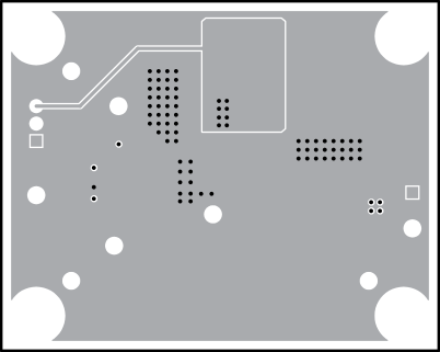 Figure 5-4 Internal Layer 2
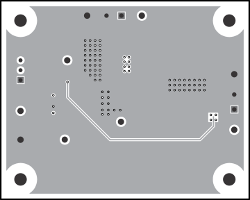 Figure 5-5 Bottom Layer