SLVU988A October 2013 – June 2021 TPS56628
3.1 Output Voltage Setpoint
To change the output voltage of the EVMs, change the value of resistor R1. Changing the value of R1 can change the output voltage more than 0.8 V. The value of R1 for a specific output voltage can be calculated using Equation 1.
For output voltage from 0.8 to 5.5 V:
Equation 1. 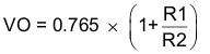
Table 3-1 lists the R1 values for some common output voltages. An option feed-forward capacitor (C4) may be used to improve phase margin. Pads for this component (C4) are provided on the printed-circuit board (PCB). Note that the resistor values given in Table 3-1 are standard values and not the exact value calculated using Equation 1.
Table 3-1 Output Voltages
| Output Voltage (V) | R1 (kΩ) | R2 (kΩ) | C4 (pF)(1) | L1 (µH) | C9 + C10 + C11 (µF) | |||||
|---|---|---|---|---|---|---|---|---|---|---|
| MIN | TYP | MAX | MIN | TYP | MAX | MIN | MAX | |||
| 1 | 6.81 | 22.1 | 5 | 150 | 220 | 1.0 | 1.5 | 4.7 | 20 | 68 |
| 1.05 | 8.25 | 22.1 | 5 | 150 | 220 | 1.0 | 1.5 | 4.7 | 20 | 68 |
| 1.2 | 12.7 | 22.1 | 5 | 100 | 1.0 | 1.5 | 4.7 | 20 | 68 | |
| 1.5 | 21.5 | 22.1 | 5 | 68 | 1.0 | 1.5 | 4.7 | 20 | 68 | |
| 1.8 | 30.1 | 22.1 | 5 | 22 | 1.2 | 1.5 | 4.7 | 20 | 68 | |
| 2.5 | 49.9 | 22.1 | 5 | 22 | 1.5 | 2.2 | 4.7 | 20 | 68 | |
| 3.3 | 73.2 | 22.1 | 2 | 22 | 1.8 | 2.2 | 4.7 | 20 | 68 | |
| 5 | 124 | 22.1 | 2 | 22 | 2.5 | 3.3 | 4.7 | 20 | 68 | |
(1) Optional