SLVU988A October   2013  – June 2021 TPS56628


  1.   Trademarks
  2. 1Introduction
  3. 2Performance Specification Summary
  4. 3Modifications
    1. 3.1 Output Voltage Setpoint
    2. 3.2 Output Filter and Closed-Loop Response
  5. 4Test Setup and Results
    1. 4.1  Input and Output Connections
    2. 4.2  Start-Up Procedure
    3. 4.3  Efficiency
    4. 4.4  Load Regulation
    5. 4.5  Line Regulation
    6. 4.6  Load Transient Response
    7. 4.7  Output Voltage Ripple
    8. 4.8  Input Voltage Ripple
    9. 4.9  Start-Up
    10. 4.10 Shut-Down
  6. 5Board Layout
    1. 5.1 Layout
  7. 6Schematic, Bill of Materials, and Reference
    1. 6.1 Schematic
    2. 6.2 Bill of Materials
    3. 6.3 Reference
  8. 7Revision History

Schematic

Figure 6-1 is the schematic for the TPS56628EVM-534.
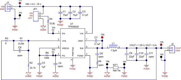
GUID-AD25DC20-386B-4FC2-A073-054257EE8BDB-low.gifFigure 6-1 TPS56628EVM-534 Schematic Diagram