SLVUBE6C November 2018 – July 2021 TPS56339
6.1 Layout
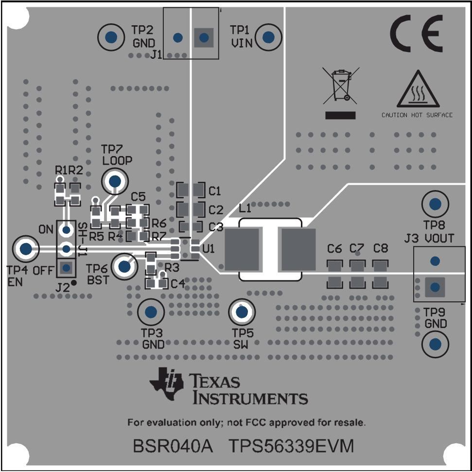
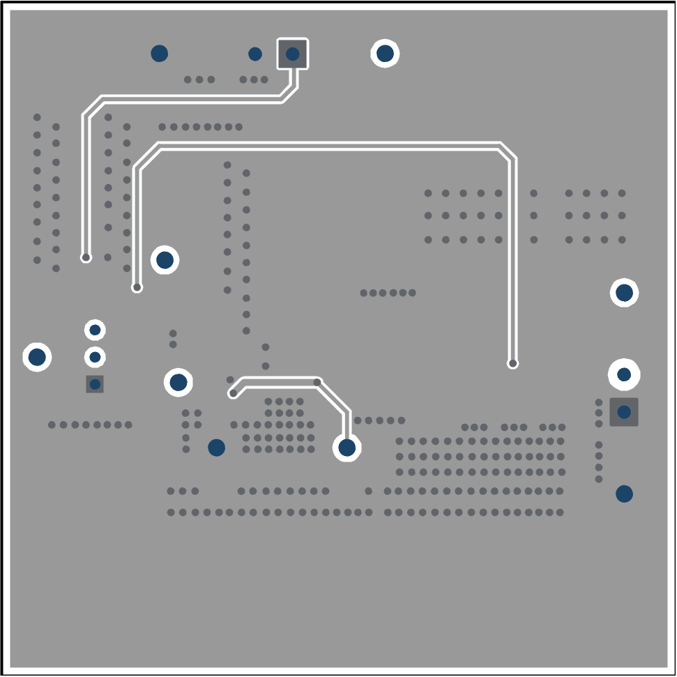
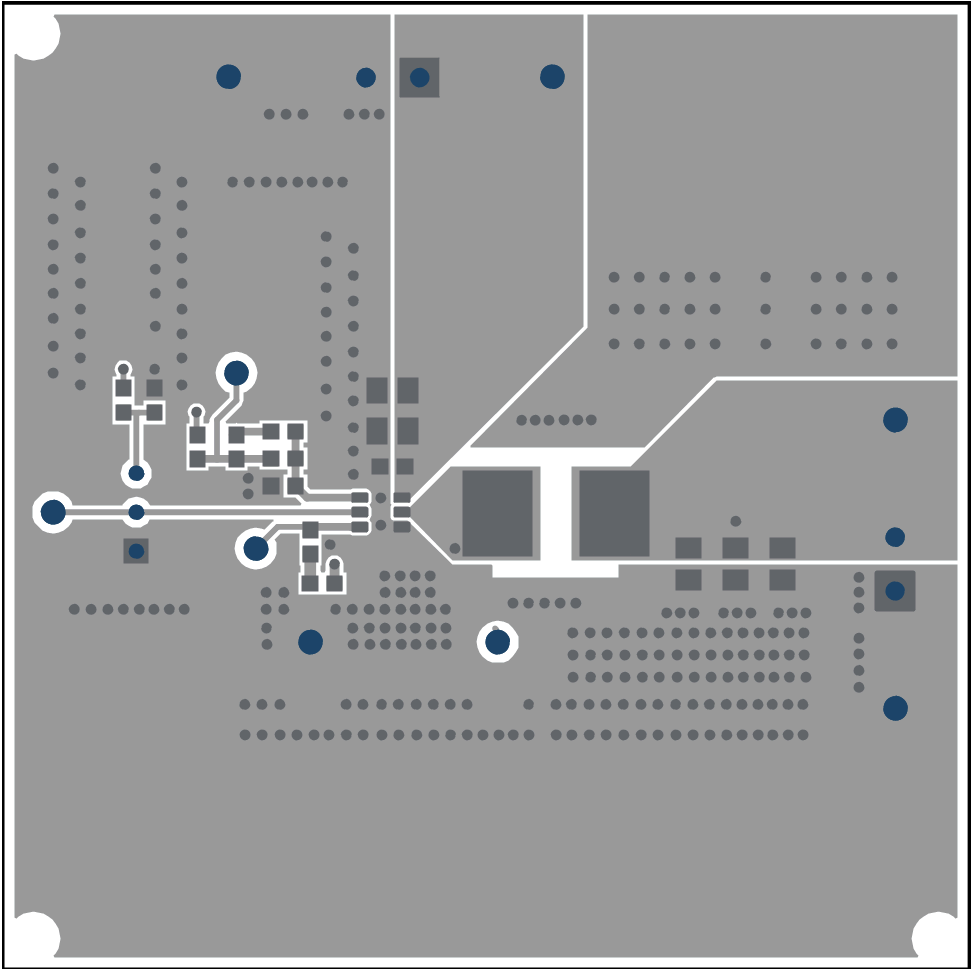
Figure 6-1,Figure 6-2 and Figure 6-3 show the board layout for the TPS56339EVM. The topside layer of the EVM is laid out in a manner typical of a user application. The top and bottom layers are 2-oz. copper.
The top layer contains the main power traces for VIN, VOUT, and SW. Also on the top layer are connections for the remaining pins of the TPS56339 and a large area filled with ground. To facilitate the placement of the main input bypass capacitor as close to the VIN and GND pins as possible. The input decoupling capacitors (C2, and C3) and bootstrap capacitor (C4) are all located as close to the IC as possible. In addition, the voltage set-point resistor divider components are also kept close to the IC. For the TPS56339, an additional input bulk capacitor may be required, depending on the EVM connection to the input supply.
 Figure 6-1 Top Assembly
 Figure 6-3 Bottom Layer
 Figure 6-2 Top Layer