SLVUBU3A April 2020 – October 2020 LM7480-Q1
- Trademarks
- 1Introduction
-
2Description
- 2.1 Input Power and Load (J1/J3 and J2/J4):
- 2.2 Enable Control (J5):
- 2.3 Over Voltage Protection (J6):
- 2.4 Input Voltage Monitor (J8 and VIN_MON):
- 2.5 Two back-back connected MOSFETs (Q1/Q3 and Q2/Q4):
- 2.6 Output slew rate control (R2 and C2):
- 2.7 Output Schottky Diode (D2) and LED indication:
- 2.8 TVS selection for 12-V battery protection:
- 2.9 TVS selection for 24-V battery protection:
- 2.10 Test Points:
- 3Schematic
- 4Test Equipment Requirements
- 5Test Setup and Results
- 6Board Layout and Bill of Materials
- 7Revision History
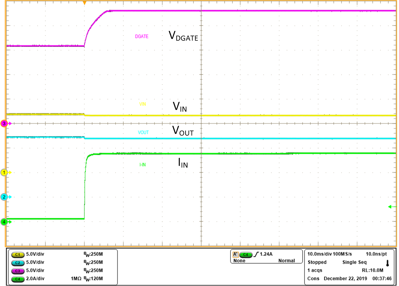
5.7 Load Response
 Figure 5-12 Load Transient Response 100 mA to 5 A